EVAL-ADUC847QS Analog Devices Inc, EVAL-ADUC847QS Datasheet - Page 44
EVAL-ADUC847QS
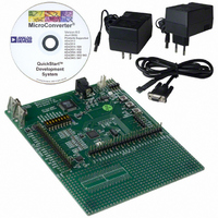
Manufacturer Part Number
EVAL-ADUC847QS
Description
KIT DEV FOR ADUC847 QUICK START
Manufacturer
Analog Devices Inc
Datasheet
1.EVAL-ADUC845QSZ.pdf
(108 pages)
Specifications of EVAL-ADUC847QS
Lead Free Status / RoHS Status
Lead free / RoHS Compliant


ADuC845/ADuC847/ADuC848
ADC0CON2 (PRIMARY ADC CHANNEL SELE
ADC0CON2 is used to select a reference source and channel for the primary ADC.
SFR Address:
Power-On Default:
Bit Addressable:
Table 26. ADC0CON2 SFR Bit Designations
Bit N
7, 6
5
4
3, 2, 1, 0
Note that because the reference-detect does not operate on the REFIN2± pair, the REFIN2± pins can go below 1 V.
o.
Name
XREF1, XREF0
–––
–––
CH3, CH2, CH1, CH0
E6H
00H
No
Descr
Primary ADC Exte
Set by the user to enable the primary ADC to use the external reference via REFIN± or REFIN2±.
Cleared by the user to enable the primary ADC to use the internal band gap reference (V
XREF1
0
0
1
1
Not Implemented. Write Don’t Care.
Not Implemented. Write Don’t Care.
Primary ADC Channel Select Bits. Written by the user to select the primary ADC channel as follows:
CH3
0
0
0
0
0
0
0
0
1
1
1
1
1
1
1
1
iption
CH2
0
0
0
0
1
1
1
1
0
0
0
0
1
1
1
1
XREF0
0
1
0
1
CH1
0
0
1
1
0
0
1
1
0
0
1
1
0
0
1
1
rna
Internal 1.25 V Reference.
REFIN± Selected.
REFIN2± (AIN3/AIN4) Selected.
Reserved.
CT REGISTER)
l Reference Sel
CH0
0
1
0
1
0
1
0
1
0
1
0
1
0
1
0
1
Rev. B | Page 44 of 108
Selected Primary ADC Input Channel.
AIN1–AINCOM
AIN2–AINCOM
AIN3–AINCOM
AIN4–AINCOM
AIN5–AINCOM
AIN6–AINCOM
AIN7–AINCOM
AIN8–AINCOM
AIN
pack
AIN10–AINCOM (LFCSP package only; not a valid selection on the MQFP
package)
AIN1–AIN2
AIN3–AIN4
AIN5–AIN6
AIN7–AIN8
AIN
package)
AINCOM–AINCOM
9–AINCOM (LFCSP package only; not a valid selection on the MQFP
9–AIN10 (LFCSP package only; not a valid selection on the MQFP
ect
age)
Bit.
REF
= 1.25 V).
Related parts for EVAL-ADUC847QS
Image
Part Number
Description
Manufacturer
Datasheet
Request
R


Part Number:
Description:
BOARD EVAL FOR SI270X-A
Manufacturer:
Silicon Laboratories Inc
Datasheet:

Part Number:
Description:
BUCK CONV REF DESIGN KIT IP1201
Manufacturer:
International Rectifier
Datasheet:
Part Number:
Description:
BOARD DEMO SYNC DUAL BUCK CNVTER
Manufacturer:
International Rectifier
Datasheet:
Part Number:
Description:
BOARD DEMO SYNC BUCK CONVETER
Manufacturer:
International Rectifier
Datasheet:

Part Number:
Description:
EVALBOARD/EB Omnidirectional microphone - Analog
Manufacturer:
Analog Devices
Datasheet:
Part Number:
Description:
EVALBOARD/EB Omnidirectional microphone - Analog
Manufacturer:
Analog Devices
Datasheet:


Part Number:
Description:
BOARD EVAL LED DRIVER LT3756
Manufacturer:
Linear Technology
Datasheet:

Part Number:
Description:
BOARD EVAL FOR AD7741/7742
Manufacturer:
Analog Devices Inc
Datasheet:

Part Number:
Description:
±1.7g Dual-Axis IMEMS Accelerometer Evaluation Board
Manufacturer:
Analog Devices Inc
Datasheet:

Part Number:
Description:
IC MULTIPLIER ANALOG 8-SOIC T/R
Manufacturer:
Analog Devices Inc
Datasheet:

Part Number:
Description:
IC ANALOG MULTIPLIER 8-DIP
Manufacturer:
Analog Devices Inc
Datasheet:
Part Number:
Description:
IC ANALOG MULTIPLIER 8-SOIC
Manufacturer:
Analog Devices Inc
Datasheet:
Part Number:
Description:
IC ANALOG MULTIPLIER 8-DIP
Manufacturer:
Analog Devices Inc
Datasheet: