EVAL-ADUC847QS Analog Devices Inc, EVAL-ADUC847QS Datasheet - Page 43
EVAL-ADUC847QS
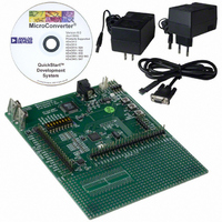
Manufacturer Part Number
EVAL-ADUC847QS
Description
KIT DEV FOR ADUC847 QUICK START
Manufacturer
Analog Devices Inc
Datasheet
1.EVAL-ADUC845QSZ.pdf
(108 pages)
Specifications of EVAL-ADUC847QS
Lead Free Status / RoHS Status
Lead free / RoHS Compliant


ADC0CON1 (PRIMARY ADC CONTROL REGISTER)
ADC0CON1 is used to configure the primary ADC for buffer, unipolar, or bipolar coding, and ADC range configuration.
SFR Address:
Power-On Def lt:
Bit Addressable:
T
Bit No.
7, 6
5
4
3
2, 1, 0
able 25. ADC0CON1 SFR Bit Designations
Name
BUF1, BUF0
UNI
–––
–––
RN2, RN1, RN0
au
D2H
07H
No
Buffer Con
BUF1
0
0
1
1
Primary AD
Set by the
Cleared by
Not Implemented. Write Don’t Care.
Not Implemented. Write Don’t Care.
Primary AD
RN2
0
0
0
0
1
1
1
1
Description
BU
0
1
0
1
RN
0
0
1
1
0
0
1
1
figuration Bits
user to enable unipolar coding; zero differential input results in 000000H output.
F0
1
the user to enable bipolar coding; zero differential input results in 800000H output.
C Unipolar Bit.
C Rang Bits. W tten by the user to select the primary ADC input range as follows:
e
RN
0
1
0
1
0
1
0
1
0
.
ri
Rev. B | Page 43 of 108
Buffer Configura
ADC0+ and ADC0− are buffered
Reserved
Buffer Bypass
Reserved
Select
±20 mV (0 mV
±40 mV (0 mV
±80 mV (0 mV
±160 m (0 m
±320 m (0 m
±640 m (0 m
±1.28
±2.56
ed
V (0
V (0
V
V
V
prim
V–1
V–2.5
ary ADC input ra
–20 mV in unipo
–40 mV in unipol
–80 mV in unipo
V–160 mV in unip
V–320 mV in unip
V–640 mV in unip
.28 V in unipolar
6 V in unipolar mode)
tion
nge (V
lar mode)
lar mode)
mode)
ar mode)
olar mode)
olar mode)
olar mode)
ADuC845/ADuC847/ADuC848
REF
= 2.5 V)
Related parts for EVAL-ADUC847QS
Image
Part Number
Description
Manufacturer
Datasheet
Request
R


Part Number:
Description:
BOARD EVAL FOR SI270X-A
Manufacturer:
Silicon Laboratories Inc
Datasheet:

Part Number:
Description:
BUCK CONV REF DESIGN KIT IP1201
Manufacturer:
International Rectifier
Datasheet:
Part Number:
Description:
BOARD DEMO SYNC DUAL BUCK CNVTER
Manufacturer:
International Rectifier
Datasheet:
Part Number:
Description:
BOARD DEMO SYNC BUCK CONVETER
Manufacturer:
International Rectifier
Datasheet:

Part Number:
Description:
EVALBOARD/EB Omnidirectional microphone - Analog
Manufacturer:
Analog Devices
Datasheet:
Part Number:
Description:
EVALBOARD/EB Omnidirectional microphone - Analog
Manufacturer:
Analog Devices
Datasheet:


Part Number:
Description:
BOARD EVAL LED DRIVER LT3756
Manufacturer:
Linear Technology
Datasheet:

Part Number:
Description:
BOARD EVAL FOR AD7741/7742
Manufacturer:
Analog Devices Inc
Datasheet:

Part Number:
Description:
±1.7g Dual-Axis IMEMS Accelerometer Evaluation Board
Manufacturer:
Analog Devices Inc
Datasheet:

Part Number:
Description:
IC MULTIPLIER ANALOG 8-SOIC T/R
Manufacturer:
Analog Devices Inc
Datasheet:

Part Number:
Description:
IC ANALOG MULTIPLIER 8-DIP
Manufacturer:
Analog Devices Inc
Datasheet:
Part Number:
Description:
IC ANALOG MULTIPLIER 8-SOIC
Manufacturer:
Analog Devices Inc
Datasheet:
Part Number:
Description:
IC ANALOG MULTIPLIER 8-DIP
Manufacturer:
Analog Devices Inc
Datasheet: