AD9777-EB Analog Devices Inc, AD9777-EB Datasheet - Page 32
AD9777-EB
Manufacturer Part Number
AD9777-EB
Description
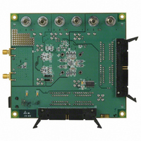
BOARD EVAL FOR AD9777
Manufacturer
Analog Devices Inc
Series
TxDAC+®r
Datasheet
1.AD9777BSVZ.pdf
(60 pages)
Specifications of AD9777-EB
Rohs Status
RoHS non-compliant
Number Of Dac's
2
Number Of Bits
16
Outputs And Type
2, Differential
Sampling Rate (per Second)
160M
Data Interface
Parallel
Settling Time
11ns
Dac Type
Current
Voltage Supply Source
Analog and Digital
Operating Temperature
-40°C ~ 85°C
Utilized Ic / Part
AD9777


AD9777
DATA AT PORTS
PLL DISABLED, ONE-PORT MODE
In one-port mode, data is received into the AD9777 as an
interleaved stream on Port 1. A clock signal (ONEPORTCLK),
running at the interleaved data rate, which is 2× the input data
rate of the internal I and Q channels, is available for data
synchronization at Pin 32.
With PLL disabled, a clock at the DAC output rate must be applied
to CLKIN. Internal dividers synthesize the ONEPORTCLK signal
at Pin 32. The selection of the data for the I or Q channel is deter-
mined by the state of the logic level applied to Pin 31 (IQSEL when
the AD9777 is in one-port mode) on the rising edge of
ONEPORTCLK. Under these conditions, IQSEL = 0 latches the
data into the I channel on the clock rising edge, while IQSEL = 1
latches the data into the Q channel. It is possible to invert the I and
Q selection by setting Control Register 02h, Bit 1 to the invert state
(Logic 1). Figure 56 illustrates the timing requirements for the data
inputs as well as the IQSEL input. Note that the 1× interpolation
rate is not available in the one-port mode.
One-port mode is very useful when interfacing with devices,
such as the Analog Devices AD6622 or AD6623 transmit signal
processors, in which two digital data channels have been inter-
leaved (multiplexed). The programmable modes’ ONEPORTCLK
inversion, ONEPORTCLK driver strength, and IQ pairing
described in the PLL Enabled, One-Port Mode section have
identical functionality with the PLL disable.
Figure 55. Timing Requirements in Two-Port Input Mode, with PLL Disabled
1 AND 2
DATACLK
CLKIN
t
OD
t
S
t
H
t
t
t
OD
S
H
= 5.0ns (MAX)
= –3.2ns (MAX)
= 6.5ns (MIN) TO 8.0ns (MAX)
Rev. C | Page 32 of 60
INPUT DATA AT PORT 1
t
t
t
t
t
t
(TYP SPECS)
DIGITAL FILTER MODES
The I and Q data paths of the AD9777 have their own
independent half-band FIR filters. Each data path consists of
three FIR filters, providing up to 8× interpolation for each
channel. The rate of interpolation is determined by the state of
Control Register 01h, Bit 7 and Bit 6. Figure 2 to Figure 4 show
the response of the digital filters when the AD9777 is set to 2×,
4×, and 8× modes. The frequency axes of these graphs have
been normalized to the input data rate of the DAC. As the
graphs show, the digital filters can provide greater than 75 dB of
out-of-band rejection.
An online tool is available for quick and easy analysis of the
AD9777 interpolation filters in the various modes. The link can be
accessed at http://www.analog.com/Analog_Root/static/
techsupport/designtools/interactiveTools/dac/ad9777image.html.
AMPLITUDE MODULATION
Given two sine waves at the same frequency but with a 90°
phase difference, a point of view in time can be taken such that
the waveform that leads in phase is cosinusoidal and the
waveform that lags is sinusoidal. Analysis of complex variables
states that the cosine waveform can be defined as having real
positive and negative frequency components, while the sine
waveform consists of imaginary positive and negative frequency
images. This is shown graphically in the frequency domain in
Figure 57.
I AND Q INTERLEAVED
OD
OD
S
H
IQS
IQH
Figure 56. Timing Requirements in One-Port Input Mode, with PLL Disabled
= 3.0ns (MAX)
= –1.0ns (MAX)
= 4.0ns (MIN)
= 4.7ns (MAX)
= 3.5ns (MAX)
= –1.5ns (MAX)
TO 5.5ns (MAX)
ONEPORTCLK
CLKIN
IQSEL
t
IQS
t
OD
t
S
t
H
t
IQH
Related parts for AD9777-EB
Image
Part Number
Description
Manufacturer
Datasheet
Request
R

Part Number:
Description:
16Bit 400 MSPS Dual TxDAC+ D/A Converter
Manufacturer:
Analog Devices Inc
Datasheet:

Part Number:
Description:
±1.7g Dual-Axis IMEMS Accelerometer Evaluation Board
Manufacturer:
Analog Devices Inc
Datasheet:
Part Number:
Description:
Inertial Sensor Evaluation System
Manufacturer:
Analog Devices Inc
Datasheet:
Part Number:
Description:
Manufacturer:
Analog Devices Inc
Datasheet:
Part Number:
Description:
Manufacturer:
Analog Devices Inc
Datasheet:
Part Number:
Description:
Manufacturer:
Analog Devices Inc
Datasheet:
Part Number:
Description:
Manufacturer:
Analog Devices Inc
Datasheet:
Part Number:
Description:
Manufacturer:
Analog Devices Inc
Datasheet:
Part Number:
Description:
Manufacturer:
Analog Devices Inc
Datasheet:
Part Number:
Description:
Manufacturer:
Analog Devices Inc
Datasheet:
Part Number:
Description:
Manufacturer:
Analog Devices Inc
Datasheet:
Part Number:
Description:
Manufacturer:
Analog Devices Inc
Datasheet:
Part Number:
Description:
Manufacturer:
Analog Devices Inc
Datasheet: