AD9777-EB Analog Devices Inc, AD9777-EB Datasheet - Page 27
AD9777-EB
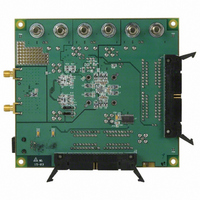
Manufacturer Part Number
AD9777-EB
Description
BOARD EVAL FOR AD9777
Manufacturer
Analog Devices Inc
Series
TxDAC+®r
Datasheet
1.AD9777BSVZ.pdf
(60 pages)
Specifications of AD9777-EB
Rohs Status
RoHS non-compliant
Number Of Dac's
2
Number Of Bits
16
Outputs And Type
2, Differential
Sampling Rate (per Second)
160M
Data Interface
Parallel
Settling Time
11ns
Dac Type
Current
Voltage Supply Source
Analog and Digital
Operating Temperature
-40°C ~ 85°C
Utilized Ic / Part
AD9777


A configuration for differentially driving the clock inputs is
given in Figure 44. DC-blocking capacitors can be used to
couple a clock driver output whose voltage swings exceed
CLKVDD or CLKGND. If the driver voltage swings are within
the supply range of the AD9777, the dc-blocking capacitors and
bias resistors are not necessary.
A transformer, such as the T1-1T from Mini-Circuits, can also
be used to convert a single-ended clock to differential. This
method is used on the AD9777 evaluation board so that an
external sine wave with no dc offset can be used as a differential
clock.
PECL/ECL drivers require varying termination networks, the
details of which are left out of Figure 43 and Figure 44 but can
be found in application notes such as AND8020/D from On
Semiconductor. These networks depend on the assumed
transmission line impedance and power supply voltage of the
clock driver. Optimum performance of the AD9777 is achieved
when the driver is placed very close to the AD9777 clock inputs,
thereby negating any transmission line effects such as reflec-
tions due to mismatch.
The quality of the clock and data input signals is important in
achieving optimum performance. The external clock driver
circuitry should provide the AD9777 with a low jitter clock
input that meets the minimum/maximum logic levels while
providing fast edges. Although fast clock edges help minimize
any jitter that manifests itself as phase noise on a reconstructed
waveform, the high gain bandwidth product of the AD9777’s
clock input comparator can tolerate differential sine wave inputs
as low as 0.5 V p-p with minimal degradation of the output
noise floor.
Figure 44. Differential Clock Driving Clock Inputs
ECL/PECL
AD9777
0.1µF
0.1µF
0.1µF
1kΩ
1kΩ
1kΩ
1kΩ
CLK+
CLKVDD
CLK–
CLKGND
Rev. C | Page 27 of 60
PROGRAMMABLE PLL
CLKIN can function either as an input data rate clock (PLL
enabled) or as a DAC data rate clock (PLL disabled) according
to the state of Address 02h, Bit 7 in the SPI port register. The
internal operation of the AD9777 clock circuitry in these two
modes is illustrated in Figure 45 and Figure 46.
The PLL clock multiplier and distribution circuitry produce the
necessary internal synchronized 1×, 2×, 4×, and 8× clocks for
the rising edge triggered latches, interpolation filters,
modulators, and DACs. This circuitry consists of a phase
detector, charge pump, voltage controlled oscillator (VCO),
prescaler, clock distribution, and SPI port control. The charge
pump, VCO, differential clock input buffer, phase detector,
prescaler, and clock distribution are all powered from
CLKVDD. PLL lock status is indicated by the logic signal at the
PLL_LOCK pin, as well as by the status of Bit 1, Register 00h.
To ensure optimum phase noise performance from the PLL
clock multiplier and distribution, CLKVDD should originate
from a clean analog supply. Table 10 defines the minimum
input data rates versus the interpolation and PLL divider
setting. If the input data rate drops below the defined minimum
under these conditions, VCO phase noise can increase
significantly. The VCO speed is a function of the input data
rate, the interpolation rate, and the VCO prescaler, according to
the following function:
LATCHES
INTERPOLATION
CONTROL
INPUT
DATA
RATE
VCO
Input
1
Speed
Figure 45. PLL and Clock Circuitry with PLL Enabled
2
Data
0 = NO LOCK
PLL_LOCK
DISTRIBUTION
INTERPOLATION
1 = LOCK
MODULATORS,
INTERNAL SPI
CIRCUITRY
REGISTERS
SPI PORT
4
AND DACS
CONTROL
CLOCK
FILTERS,
(
Rate
MHz
8
(
MHz
)
=
CLK+
MODULATION
CONTROL
)
×
RATE
Interpolat
CLK–
PRESCALER
DETECTOR
PHASE
AD9777
ion
CONTROL
(PLL ON)
(PRESCALER)
PLL DIVIDER
PLL
Rate
CONTROL
CHARGE
PUMP
VCO
PLLVDD
×
Prescaler
AD9777
LPF
Related parts for AD9777-EB
Image
Part Number
Description
Manufacturer
Datasheet
Request
R

Part Number:
Description:
16Bit 400 MSPS Dual TxDAC+ D/A Converter
Manufacturer:
Analog Devices Inc
Datasheet:

Part Number:
Description:
±1.7g Dual-Axis IMEMS Accelerometer Evaluation Board
Manufacturer:
Analog Devices Inc
Datasheet:
Part Number:
Description:
Inertial Sensor Evaluation System
Manufacturer:
Analog Devices Inc
Datasheet:
Part Number:
Description:
Manufacturer:
Analog Devices Inc
Datasheet:
Part Number:
Description:
Manufacturer:
Analog Devices Inc
Datasheet:
Part Number:
Description:
Manufacturer:
Analog Devices Inc
Datasheet:
Part Number:
Description:
Manufacturer:
Analog Devices Inc
Datasheet:
Part Number:
Description:
Manufacturer:
Analog Devices Inc
Datasheet:
Part Number:
Description:
Manufacturer:
Analog Devices Inc
Datasheet:
Part Number:
Description:
Manufacturer:
Analog Devices Inc
Datasheet:
Part Number:
Description:
Manufacturer:
Analog Devices Inc
Datasheet:
Part Number:
Description:
Manufacturer:
Analog Devices Inc
Datasheet:
Part Number:
Description:
Manufacturer:
Analog Devices Inc
Datasheet: