AD9777-EB Analog Devices Inc, AD9777-EB Datasheet - Page 30
AD9777-EB
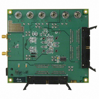
Manufacturer Part Number
AD9777-EB
Description
BOARD EVAL FOR AD9777
Manufacturer
Analog Devices Inc
Series
TxDAC+®r
Datasheet
1.AD9777BSVZ.pdf
(60 pages)
Specifications of AD9777-EB
Rohs Status
RoHS non-compliant
Number Of Dac's
2
Number Of Bits
16
Outputs And Type
2, Differential
Sampling Rate (per Second)
160M
Data Interface
Parallel
Settling Time
11ns
Dac Type
Current
Voltage Supply Source
Analog and Digital
Operating Temperature
-40°C ~ 85°C
Utilized Ic / Part
AD9777


AD9777
Register 3, Bit 7 = 1, Register 1, Bit 0 = 0; PLL lock indicator out
of Pin 53.
Register 3, Bit 7 = 0, Register 1, Bit 0 = 1; DATACLK out of Pin 8.
Register 3, Bit 7 = 1, Register 1, Bit 0 = 1; DATACLK out of Pin 53.
In one-port mode, P2B14 and P2B15 from input data port two
are redefined as IQSEL and ONEPORTCLK, respectively. The
input data in one-port mode is steered to one of the two inter-
nal data channels based on the logic level of IQSEL. A clock
signal, ONEPORTCLK, is generated by the AD9777 in this
mode for the purpose of data synchronization. ONEPORTCLK
runs at the input interleaved data rate, which is 2× the data rate
at the internal input to either channel.
Test configurations showing the various clocks that are required
and generated by the AD9777 with the PLL enabled/disabled
and in the one-port/two-port modes are given in Figure 101 to
Figure 104. Jumper positions needed to operate the AD9777
evaluation board in these modes are given as well.
PLL ENABLED, TWO-PORT MODE
(Control Register 02h, Bits 6 to 0 and 04h, Bits 7 to 1)
With the phase-locked loop (PLL) enabled and the AD9777 in
two-port mode, the speed of CLKIN is inherently that of the
input data rate. In two-port mode, Pin 8 (DATACLK/PLL_
LOCK) can be programmed (Control Register 01h, Bit 0) to
function as either a lock indicator for the internal PLL or as a
clock running at the input data rate. When Pin 8 is used as a
clock output (DATACLK), its frequency is equal to that of
CLKIN. Data at the input ports is latched into the AD9777 on
the rising edge of the CLKIN. Figure 52 shows the delay, t
inherent between the rising edge of CLKIN and the rising edge
of DATACLK, as well as the setup and hold requirements for
the data at Ports 1 and 2. The setup and hold times given in Figure
52 are the input data transitions with respect to CLKIN. Note
that in two-port mode (PLL enabled or disabled), the data rate
at the interpolation filter inputs is the same as the input data
rate at Port 1 and Port 2.
The DAC output sample rate in two-port mode is equal to the
clock input rate multiplied by the interpolation rate. If zero
stuffing is used, another factor of 2 must be included to
calculate the DAC sample rate.
DATACLK INVERSION
(Control Register 02h, Bit 4)
By programming this bit, the DATACLK signal shown in Figure 53
can be inverted. With inversion enabled, t
between the rising edge of CLKIN and the falling edge of
DATACLK. No other effect on timing occurs.
OD
refers to the time
OD
,
Rev. C | Page 30 of 60
DATA AT PORTS
DATACLK DRIVER STRENGTH
(Control Register 02h, Bit 5)
The DATACLK output driver strength is capable of driving
>10 mA into a 330 Ω load while providing a rise time of 3 ns.
Figure 53 shows DATACLK driving a 330 Ω resistive load at a
frequency of 50 MHz. By enabling the drive strength option
(Control Register 02h, Bit 5), the amplitude of DATACLK under
these conditions increases by approximately 200 mV.
PLL ENABLED, ONE-PORT MODE
(Control Register 02h, Bits 6 to 1 and 04h, Bits 7 to 1)
In one-port mode, the I and Q channels receive their data from
an interleaved stream at digital input Port 1. The function of
Pin 32 is defined as an output (ONEPORTCLK) that generates a
clock at the interleaved data rate, which is 2× the internal input
data rate of the I and Q channels. The frequency of CLKIN is
equal to the internal input data rate of the I and Q channels.
Figure 52. Timing Requirements in Two-Port Input Mode with PLL Enabled
–0.5
3.0
2.5
2.0
1.5
1.0
0.5
1 AND 2
0
0
Figure 53. DATACLK Driver Capability into 330 Ω at 50 MHz
DATACLK
CLKIN
10
t
S
t
H
20
t
OD
TIME (ns)
DELTA APPROX. 2.8ns
30
t
t
S
H
= 0.0ns (MAX)
= 2.5ns (MAX)
40
50
Related parts for AD9777-EB
Image
Part Number
Description
Manufacturer
Datasheet
Request
R

Part Number:
Description:
16Bit 400 MSPS Dual TxDAC+ D/A Converter
Manufacturer:
Analog Devices Inc
Datasheet:

Part Number:
Description:
±1.7g Dual-Axis IMEMS Accelerometer Evaluation Board
Manufacturer:
Analog Devices Inc
Datasheet:
Part Number:
Description:
Inertial Sensor Evaluation System
Manufacturer:
Analog Devices Inc
Datasheet:
Part Number:
Description:
Manufacturer:
Analog Devices Inc
Datasheet:
Part Number:
Description:
Manufacturer:
Analog Devices Inc
Datasheet:
Part Number:
Description:
Manufacturer:
Analog Devices Inc
Datasheet:
Part Number:
Description:
Manufacturer:
Analog Devices Inc
Datasheet:
Part Number:
Description:
Manufacturer:
Analog Devices Inc
Datasheet:
Part Number:
Description:
Manufacturer:
Analog Devices Inc
Datasheet:
Part Number:
Description:
Manufacturer:
Analog Devices Inc
Datasheet:
Part Number:
Description:
Manufacturer:
Analog Devices Inc
Datasheet:
Part Number:
Description:
Manufacturer:
Analog Devices Inc
Datasheet:
Part Number:
Description:
Manufacturer:
Analog Devices Inc
Datasheet: