AD9777-EB Analog Devices Inc, AD9777-EB Datasheet - Page 28
AD9777-EB
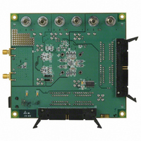
Manufacturer Part Number
AD9777-EB
Description
BOARD EVAL FOR AD9777
Manufacturer
Analog Devices Inc
Series
TxDAC+®r
Datasheet
1.AD9777BSVZ.pdf
(60 pages)
Specifications of AD9777-EB
Rohs Status
RoHS non-compliant
Number Of Dac's
2
Number Of Bits
16
Outputs And Type
2, Differential
Sampling Rate (per Second)
160M
Data Interface
Parallel
Settling Time
11ns
Dac Type
Current
Voltage Supply Source
Analog and Digital
Operating Temperature
-40°C ~ 85°C
Utilized Ic / Part
AD9777


AD9777
LATCHES
In addition, if the zero stuffing option is enabled, the VCO doubles its
speed again. Phase noise can be slightly higher with the PLL enabled.
Figure 47 illustrates typical phase noise performance of the AD9777
with 2× interpolation and various input data rates. The signal
synthesized for the phase noise measurement was a single carrier at a
frequency of f
quantization noise and distortion spurs as a factor in the measure-
ment. Although the curves blend in Figure 47, the different
conditions are given for clarity in the table preceding Figure 47.
Figure 47 also contains a table detailing PLL divider settings vs.
interpolation rate and maximum and minimum f
maximum f
data rate of the AD9777. However, maximum rates of less than 160
MSPS and all minimum f
mum speeds of the internal PLL VCO. Figure 48 shows typical
performance of the PLL lock signal (Pin 8 or Pin 53) when the PLL is
in the process of locking.
Table 10. PLL Optimization
Interpolation
Rate
1
1
1
1
2
2
2
2
4
4
4
4
8
8
8
8
INTERPOLATION
CONTROL
INPUT
DATA
RATE
1
Figure 46. PLL and Clock Circuitry with PLL Disabled
DATA
2
0 = NO LOCK
DATA
PLL_LOCK
DISTRIBUTION
INTERPOLATION
1 = LOCK
MODULATORS,
INTERNAL SPI
CIRCUITRY
rates of 160 MSPS are due to the maximum input
REGISTERS
SPI PORT
4
AND DACS
CONTROL
CLOCK
/4. The repetitive nature of this signal eliminates
FILTERS,
8
Divider
Setting
1
2
4
8
1
2
4
8
1
2
4
8
1
2
4
8
DATA
CLK+
MODULATION
rates are due to maximum and mini-
CONTROL
RATE
CLK–
PRESCALER
DETECTOR
Minimum
f
32
16
8
4
24
12
6
3
24
12
6
3
24
12
6
3
PHASE
DATA
CONTROL
(PLL ON)
(PRESCALER)
AD9777
PLL DIVIDER
PLL
CONTROL
DATA
CHARGE
PUMP
VCO
rates. Note that
Maximum
f
160
160
112
56
160
112
56
28
100
56
28
14
50
28
14
7
DATA
Rev. C | Page 28 of 60
Table 11. Required PLL Prescaler Ration vs. f
f
125
125
100
75
50
It is important to note that the resistor/capacitor needed for the
PLL loop filter is internal on the AD9777. This suffices unless
the input data rate is below 10 MHz, in which case an external
series RC is required between the LPF and CLKVDD pins.
DATA
–100
–110
Figure 48. PLL_LOCK Output Signal (Pin 8) in the Process of Locking
–10
–20
–30
–40
–50
–60
–70
–80
–90
(MSPS)
0
0
1
Figure 47. Phase Noise Performance
PLL
Disabled
Enabled
Enabled
Enabled
Enabled
FREQUENCY OFFSET (MHz)
(Typical Lock Time)
2
3
Prescaler Ratio
Div 1
Div 2
Div 2
Div 4
4
DATA
5
Related parts for AD9777-EB
Image
Part Number
Description
Manufacturer
Datasheet
Request
R

Part Number:
Description:
16Bit 400 MSPS Dual TxDAC+ D/A Converter
Manufacturer:
Analog Devices Inc
Datasheet:

Part Number:
Description:
±1.7g Dual-Axis IMEMS Accelerometer Evaluation Board
Manufacturer:
Analog Devices Inc
Datasheet:
Part Number:
Description:
Inertial Sensor Evaluation System
Manufacturer:
Analog Devices Inc
Datasheet:
Part Number:
Description:
Manufacturer:
Analog Devices Inc
Datasheet:
Part Number:
Description:
Manufacturer:
Analog Devices Inc
Datasheet:
Part Number:
Description:
Manufacturer:
Analog Devices Inc
Datasheet:
Part Number:
Description:
Manufacturer:
Analog Devices Inc
Datasheet:
Part Number:
Description:
Manufacturer:
Analog Devices Inc
Datasheet:
Part Number:
Description:
Manufacturer:
Analog Devices Inc
Datasheet:
Part Number:
Description:
Manufacturer:
Analog Devices Inc
Datasheet:
Part Number:
Description:
Manufacturer:
Analog Devices Inc
Datasheet:
Part Number:
Description:
Manufacturer:
Analog Devices Inc
Datasheet:
Part Number:
Description:
Manufacturer:
Analog Devices Inc
Datasheet: