AD9777-EB Analog Devices Inc, AD9777-EB Datasheet - Page 21
AD9777-EB
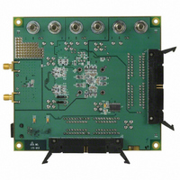
Manufacturer Part Number
AD9777-EB
Description
BOARD EVAL FOR AD9777
Manufacturer
Analog Devices Inc
Series
TxDAC+®r
Datasheet
1.AD9777BSVZ.pdf
(60 pages)
Specifications of AD9777-EB
Rohs Status
RoHS non-compliant
Number Of Dac's
2
Number Of Bits
16
Outputs And Type
2, Differential
Sampling Rate (per Second)
160M
Data Interface
Parallel
Settling Time
11ns
Dac Type
Current
Voltage Supply Source
Analog and Digital
Operating Temperature
-40°C ~ 85°C
Utilized Ic / Part
AD9777


Address 03h
Bit 7: This allows the data rate clock (divided down from the
DAC clock) to be output at either the DATACLK/PLL_LOCK
pin (Pin 8) or at the SPI_SDO pin (Pin 53). The default of 0 in
this register enables the data rate clock at DATACLK/
PLL_LOCK, while a 1 in this register causes the data rate clock
to be output at SPI_SDO. For more information, see the Two
Port Data Input Mode section.
Bit 1, Bit 0: Setting this divide ratio to a higher number allows
the VCO in the PLL to run at a high rate (for best performance)
while the DAC input and output clocks run substantially slower.
The divider ratio is set according to the following table.
00
01
10
11
Address 04h
Bit 7: Logic 0 (default) disables the internal PLL. Logic 1
enables the PLL.
Bit 6: Logic 0 (default) sets the charge pump control to
automatic. In this mode, the charge pump bias current is
controlled by the divider ratio defined in Address 03h, Bits 1
and 0. Logic 1 allows the user to manually define the charge
pump bias current using Address 04h, Bits 2, 1, and 0. Adjusting
the charge pump bias current allows the user to optimize the
noise/settling performance of the PLL.
Bit 2, Bit 1, Bit 0: With the charge pump control set to manual,
these bits define the charge pump bias current according to the
following table.
000
001
010
011
111
I
I
I
OUTA
OUTB
OFFSET
=
=
=
⎡
⎢
⎣
⎡
⎢
⎣
⎛ ×
⎜
⎝
⎛ ×
⎜
⎝
4
6
6
×
I
8
I
8
I
REF
÷1
÷2
÷4
÷8
50 µA
100 µA
200 µA
400 µA
800 µA
REF
REF
⎛
⎜
⎝
OFFSET
⎞
⎟
⎠
⎞
⎟
⎠
⎛
⎜
⎝
⎛
⎜
⎝
1024
COARSE
COARSE
16
16
⎞
⎟
⎠
(
A
+
+
)
1
1
⎞
⎟
⎠
⎞
⎟
⎠
−
−
⎛ ×
⎜
⎝
⎛ ×
⎜
⎝
3
3
32
32
I
I
REF
REF
⎞
⎟
⎠
⎞
⎟
⎠
⎛
⎜
⎝
⎛
⎜
⎝
FINE
FINE
256
256
⎞
⎟
⎠
⎞
⎟
⎠
⎤
⎥
⎦
⎤
⎥
⎦
Rev. C | Page 21 of 60
×
×
⎡
⎢
⎢
⎣
⎡
⎢
⎣
⎛
⎜
⎝
⎛
⎜
⎝
1024
1024
24
24
⎞
⎟
⎠
⎞
⎟
⎠
⎛
⎜ ⎜
⎝
⎛
⎜
⎝
2
DATA
Address 05h, 09h
Bit 7, Bit 6, Bit 5, Bit 4, Bit 3, Bit 2, Bit 1, and Bit 0: These bits
represent an 8-bit binary number (Bit 7 MSB) that defines the
fine gain adjustment of the I (05h) and Q (09h) DAC according
to Equation 1.
Address 06h, 0Ah
Bit 3, Bit 2, Bit 1, and Bit 0: These bits represent a 4-bit binary
number (Bit 3 MSB) that defines the coarse gain adjustment of
the I (06h) and Q (0Ah) DACs according to Equation 1.
Address 07h, 0Bh
Bit 7, Bit 6, Bit 5, Bit 4, Bit 3, Bit 2, Bit 1, and Bit 0: These bits
are used in conjunction with Address 08h, 0Ch, Bits 1, 0.
Address 08h, 0Ch
Bit 1 and Bit 0: The 10 bits from these two address pairs (07h,
08h and 0Bh, 0Ch) represent a 10-bit binary number that
defines the offset adjustment of the I and Q DACs according to
Equation 1. (07h, 0Bh–Bit 7 MSB/08h, 0Ch–Bit 0 LSB).
Address 08h, 0Ch
Bit 7: This bit determines the direction of the offset of the I
(08h) and Q (0Ch) DACs. A Logic 0 applies a positive offset
current to I
to I
bits in Addresses 07h, 0Bh, 08h, 0Ch according to Equation 1.
Equation 1 shows I
coarse gain, and offset adjustment when using 2R mode. In 1R
mode, the current I
(Pin 60). This current is divided equally into each channel so that
a scaling factor of one-half must be added to these equations for
full-scale currents for both DACs and the offset.
16
2
16
−
OUTB
DATA
2
16
⎞
⎟
⎠
. The magnitude of the offset current is defined by the
⎤
⎥
⎦
(
A
)
OUTA
−
1
⎞
⎟ ⎟
⎠
, while a Logic 1 applies a positive offset current
⎤
⎥
⎥
⎦
(
A
REF
OUTA
)
is created by a single FSADJ resistor
and I
OUTB
as a function of fine gain,
AD9777
(1)
Related parts for AD9777-EB
Image
Part Number
Description
Manufacturer
Datasheet
Request
R

Part Number:
Description:
16Bit 400 MSPS Dual TxDAC+ D/A Converter
Manufacturer:
Analog Devices Inc
Datasheet:

Part Number:
Description:
±1.7g Dual-Axis IMEMS Accelerometer Evaluation Board
Manufacturer:
Analog Devices Inc
Datasheet:
Part Number:
Description:
Inertial Sensor Evaluation System
Manufacturer:
Analog Devices Inc
Datasheet:
Part Number:
Description:
Manufacturer:
Analog Devices Inc
Datasheet:
Part Number:
Description:
Manufacturer:
Analog Devices Inc
Datasheet:
Part Number:
Description:
Manufacturer:
Analog Devices Inc
Datasheet:
Part Number:
Description:
Manufacturer:
Analog Devices Inc
Datasheet:
Part Number:
Description:
Manufacturer:
Analog Devices Inc
Datasheet:
Part Number:
Description:
Manufacturer:
Analog Devices Inc
Datasheet:
Part Number:
Description:
Manufacturer:
Analog Devices Inc
Datasheet:
Part Number:
Description:
Manufacturer:
Analog Devices Inc
Datasheet:
Part Number:
Description:
Manufacturer:
Analog Devices Inc
Datasheet:
Part Number:
Description:
Manufacturer:
Analog Devices Inc
Datasheet: