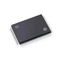
C8051F060-TB Silicon Laboratories Inc, C8051F060-TB Datasheet - Page 58

C8051F060-TB
Manufacturer Part Number
C8051F060-TB
Description
BOARD PROTOTYPING W/C8051F060
Manufacturer
Silicon Laboratories Inc
Type
MCUr
Specifications of C8051F060-TB
Contents
Board
Processor To Be Evaluated
C8051F06x
Interface Type
USB
Lead Free Status / RoHS Status
Contains lead / RoHS non-compliant
For Use With/related Products
C8051F060
Lead Free Status / Rohs Status
Lead free / RoHS Compliant
- Current page: 58 of 328
- Download datasheet (2Mb)
C8051F060/1/2/3/4/5/6/7
58
Bits 7-4: AD0SC3-0: ADC0 SAR Conversion Clock Period Bits.
Bit 3:
Bit 2:
Bit 1:
Bit 0:
AD0SC3
R/W
Bit7
SAR Conversion clock is divided down from the system clock according to the AD0SC bits
(AD0SC3-0). The number of system clocks used for each SAR conversion clock is equal to
AD0SC + 1. (Note: the ADC0 SAR Conversion Clock should be less than or equal to
25 MHz). See Table 5.1 for conversion timing details.
AD0SCAL: System Calibration Enable.
0: Internal ground and reference voltage are used during offset and gain calibration.
1: External voltages can be used during offset and gain calibration.
AD0GCAL: Gain Calibration.
Read:
0: Gain Calibration is completed or not yet started.
1: Gain Calibration is in progress.
Write:
0: No Effect.
1: Initiates a gain calibration if ADC0 is idle.
AD0LCAL: Linearity Calibration
Read
0: Linearity Calibration is completed or not yet started
1: Linearity Calibration is in progress
Write
0: No Effect
1: Initiates a linearity calibration if ADC0 is idle
AD0OCAL: Offset Calibration.
Read:
0: Offset Calibration is completed or not yet started.
1: Offset Calibration is in progress.
Write:
0: No Effect.
1: Initiates an offset calibration if ADC0 is idle.
AD0SC2
R/W
Bit6
Figure 5.7. ADC0CF: ADC0 Configuration Register
AD0SC1
R/W
Bit5
AD0SC0
R/W
Bit4
AD0SCAL AD0GCAL AD0LCAL
Rev. 1.2
R/W
Bit3
R/W
Bit2
R/W
Bit1
SFR Address:
AD0OCAL
SFR Page:
R/W
Bit0
0xBC
0
Reset Value
11110000
Related parts for C8051F060-TB
Image
Part Number
Description
Manufacturer
Datasheet
Request
R
Part Number:
Description:
SMD/C°/SINGLE-ENDED OUTPUT SILICON OSCILLATOR
Manufacturer:
Silicon Laboratories Inc
Part Number:
Description:
Manufacturer:
Silicon Laboratories Inc
Datasheet:
Part Number:
Description:
N/A N/A/SI4010 AES KEYFOB DEMO WITH LCD RX
Manufacturer:
Silicon Laboratories Inc
Datasheet:
Part Number:
Description:
N/A N/A/SI4010 SIMPLIFIED KEY FOB DEMO WITH LED RX
Manufacturer:
Silicon Laboratories Inc
Datasheet:
Part Number:
Description:
N/A/-40 TO 85 OC/EZLINK MODULE; F930/4432 HIGH BAND (REV E/B1)
Manufacturer:
Silicon Laboratories Inc
Part Number:
Description:
EZLink Module; F930/4432 Low Band (rev e/B1)
Manufacturer:
Silicon Laboratories Inc
Part Number:
Description:
I°/4460 10 DBM RADIO TEST CARD 434 MHZ
Manufacturer:
Silicon Laboratories Inc
Part Number:
Description:
I°/4461 14 DBM RADIO TEST CARD 868 MHZ
Manufacturer:
Silicon Laboratories Inc
Part Number:
Description:
I°/4463 20 DBM RFSWITCH RADIO TEST CARD 460 MHZ
Manufacturer:
Silicon Laboratories Inc
Part Number:
Description:
I°/4463 20 DBM RADIO TEST CARD 868 MHZ
Manufacturer:
Silicon Laboratories Inc
Part Number:
Description:
I°/4463 27 DBM RADIO TEST CARD 868 MHZ
Manufacturer:
Silicon Laboratories Inc
Part Number:
Description:
I°/4463 SKYWORKS 30 DBM RADIO TEST CARD 915 MHZ
Manufacturer:
Silicon Laboratories Inc
Part Number:
Description:
N/A N/A/-40 TO 85 OC/4463 RFMD 30 DBM RADIO TEST CARD 915 MHZ
Manufacturer:
Silicon Laboratories Inc
Part Number:
Description:
I°/4463 20 DBM RADIO TEST CARD 169 MHZ
Manufacturer:
Silicon Laboratories Inc


