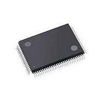
C8051F060-TB Silicon Laboratories Inc, C8051F060-TB Datasheet - Page 203

C8051F060-TB
Manufacturer Part Number
C8051F060-TB
Description
BOARD PROTOTYPING W/C8051F060
Manufacturer
Silicon Laboratories Inc
Type
MCUr
Specifications of C8051F060-TB
Contents
Board
Processor To Be Evaluated
C8051F06x
Interface Type
USB
Lead Free Status / RoHS Status
Contains lead / RoHS non-compliant
For Use With/related Products
C8051F060
Lead Free Status / Rohs Status
Lead free / RoHS Compliant
- Current page: 203 of 328
- Download datasheet (2Mb)
18.
The C8051F06x family of devices are fully integrated mixed-signal System on a Chip MCUs with 59 digital
I/O pins (C8051F060/2/4/6) or 24 digital I/O pins (C8051F061/3/5/7), organized as 8-bit Ports. All ports are
both bit- and byte-addressable through their corresponding Port Data registers. All Port pins support con-
figurable Open-Drain or Push-Pull output modes and weak pull-ups. Additionally, Port 0 pins are 5 V-toler-
ant. A block diagram of the Port I/O cell is shown in Figure 18.1. Complete Electrical Specifications for the
Port I/O pins are given in Table 18.1.
VDD = 2.7 to 3.6 V, -40 to +85 °C unless otherwise specified.
Parameter
Output High Voltage
(V
Output Low Voltage
(V
Input High Voltage (VIH)
Input Low Voltage (VIL)
Input Leakage Current
Input Capacitance
OH
OL
PORT-INPUT
/WEAK-PULLUP
PUSH-PULL
/PORT-OUTENABLE
PORT-OUTPUT
ANALOG INPUT
)
)
Port Input/Output
Analog Select
(Port 1 and 2 Only)
Conditions
I
I
I
I
DGND < Port Pin < VDD, Pin Tri-state
Weak Pull-up Off
Weak Pull-up On
Table 18.1. Port I/O DC Electrical Characteristics
OH
OH
OL
OL
= 8.5 mA
= 10 µA
= -3 mA, Port I/O Push-Pull
= -10 µA, Port I/O Push-Pull
Figure 18.1. Port I/O Cell Block Diagram
Rev. 1.2
C8051F060/1/2/3/4/5/6/7
DGND
0.7 x VDD
VDD
VDD - 0.7
VDD - 0.1
Min
Typ
VDD
10
5
(WEAK)
0.3 x VDD
Max
0.6
0.1
± 1
PORT
PAD
Units
µA
µA
pF
V
V
203
Related parts for C8051F060-TB
Image
Part Number
Description
Manufacturer
Datasheet
Request
R
Part Number:
Description:
SMD/C°/SINGLE-ENDED OUTPUT SILICON OSCILLATOR
Manufacturer:
Silicon Laboratories Inc
Part Number:
Description:
Manufacturer:
Silicon Laboratories Inc
Datasheet:
Part Number:
Description:
N/A N/A/SI4010 AES KEYFOB DEMO WITH LCD RX
Manufacturer:
Silicon Laboratories Inc
Datasheet:
Part Number:
Description:
N/A N/A/SI4010 SIMPLIFIED KEY FOB DEMO WITH LED RX
Manufacturer:
Silicon Laboratories Inc
Datasheet:
Part Number:
Description:
N/A/-40 TO 85 OC/EZLINK MODULE; F930/4432 HIGH BAND (REV E/B1)
Manufacturer:
Silicon Laboratories Inc
Part Number:
Description:
EZLink Module; F930/4432 Low Band (rev e/B1)
Manufacturer:
Silicon Laboratories Inc
Part Number:
Description:
I°/4460 10 DBM RADIO TEST CARD 434 MHZ
Manufacturer:
Silicon Laboratories Inc
Part Number:
Description:
I°/4461 14 DBM RADIO TEST CARD 868 MHZ
Manufacturer:
Silicon Laboratories Inc
Part Number:
Description:
I°/4463 20 DBM RFSWITCH RADIO TEST CARD 460 MHZ
Manufacturer:
Silicon Laboratories Inc
Part Number:
Description:
I°/4463 20 DBM RADIO TEST CARD 868 MHZ
Manufacturer:
Silicon Laboratories Inc
Part Number:
Description:
I°/4463 27 DBM RADIO TEST CARD 868 MHZ
Manufacturer:
Silicon Laboratories Inc
Part Number:
Description:
I°/4463 SKYWORKS 30 DBM RADIO TEST CARD 915 MHZ
Manufacturer:
Silicon Laboratories Inc
Part Number:
Description:
N/A N/A/-40 TO 85 OC/4463 RFMD 30 DBM RADIO TEST CARD 915 MHZ
Manufacturer:
Silicon Laboratories Inc
Part Number:
Description:
I°/4463 20 DBM RADIO TEST CARD 169 MHZ
Manufacturer:
Silicon Laboratories Inc


