P0304 Terasic Technologies Inc, P0304 Datasheet - Page 44
P0304
Manufacturer Part Number
P0304
Description
DE2-70 CALL FOR ACADEMIC PRICING
Manufacturer
Terasic Technologies Inc
Type
FPGAr
Datasheet
1.P0304.pdf
(93 pages)
Specifications of P0304
Contents
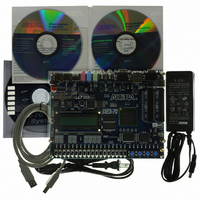
DE2-70 Board, Power Supply, Cables, Plastic cover and software
For Use With/related Products
Cyclone II 2C70
For Use With
P0033 - BOARD ADAPTER HSMC TO GPIOP0006 - BOARD ADAPTER THDB-SUMP0001 - MODULE DIGITAL CAMERA 5MP (D5M)P0307 - KIT DEV 4.3" LCD TOUCH PANEL
Lead Free Status / RoHS Status
Lead free / RoHS Compliant
Other names
DE2-70
Available stocks
Company
Part Number
Manufacturer
Quantity
Price
Company:

Part Number:
P0304UAL
Manufacturer:
Littelfuse
Quantity:
45 000
Company:
Part Number:
P0304UBL
Manufacturer:
Littelfuse
Quantity:
45 000
Company:
Part Number:
P0304UCL
Manufacturer:
Littelfuse
Quantity:
45 000


Note that the current LCD modules used on DE2/DE2-70 boards do not have backlight. Therefore
the LCD_BLON signal should not be used in users’ design projects.
5.6 Using the Expansion Header
The DE2-70 Board provides two 40-pin expansion headers. Each header connects directly to 36
pins of the Cyclone II FPGA, and also provides DC +5V (VCC5), DC +3.3V (VCC33), and two
GND pins. Among these 36 I/O pins, 4 pins are connected to the PLL clock input and output pins of
the FPGA allowing the expansion daughter cards to access the PLL blocks in the FPGA.
The voltage level of the I/O pins on the expansion headers can be adjusted to 3.3V, 2.5V, or 1.8V
using JP1. Because the expansion I/Os are connected to the BANK 5 of the FPGA and the VCCIO
voltage (VCCIO5) of this bank is controlled by the header JP1, users can use a jumper to select the
input voltage of VCCIO5 to 3.3V, 2.5V, and 1.8V to control the voltage level of the I/O pins. Table
5.7 lists the jumper settings of the JP1. The pin-outs of the JP1 appear in the Figure 5.10.
Finally, Figure 5.11 shows the related schematics. Each pin on the expansion headers is connected
to two diodes and a resistor that provide protection from high and low voltages. The figure shows
the protection circuitry for only two of the pins on each header, but this circuitry is included for all
72 data pins. Table 5.8 gives the pin assignments.
JP1 Jumper Settings
Table 5.7. Voltage level setting of the expansion headers using JP1.
LCD_DATA[5]
LCD_DATA[6]
LCD_DATA[7]
Short Pins 1 and 2
Short Pins 3 and 4
Short Pins 5 and 6
LCD_BLON
LCD_RW
LCD_ON
LCD_EN
LCD_RS
Table 5.6. Pin assignments for the LCD module.
PIN_C2
PIN_C3
PIN_G3
PIN_B2
PIN_F3
PIN_E2
PIN_F2
PIN_F1
Supplied Voltage to VCCIO5
LCD Command/Data Select, 0 = Command, 1 = Data
1.8V
2.5V
3.3V
LCD Read/Write Select, 0 = Write, 1 = Read
41
LCD Back Light ON/OFF
LCD Power ON/OFF
LCD Data[5]
LCD Data[6]
LCD Data[7]
LCD Enable
IO Voltage of Expansion
Headers (J4/J5)
1.8V
2.5V
3.3V
DE2-70 User Manual
Related parts for P0304
Image
Part Number
Description
Manufacturer
Datasheet
Request
R

Part Number:
Description:
MODULE DIGITAL CAMERA 5MP (D5M)
Manufacturer:
Terasic Technologies Inc
Datasheet:

Part Number:
Description:
USB BLASTER CABLE
Manufacturer:
Terasic Technologies Inc
Datasheet:

Part Number:
Description:
BOARD ADAPTER HSMC TO GPIO
Manufacturer:
Terasic Technologies Inc
Datasheet:

Part Number:
Description:
BOARD ADAPTER THDB-SUM
Manufacturer:
Terasic Technologies Inc
Datasheet:

Part Number:
Description:
KIT DEV 4.3" LCD TOUCH PANEL
Manufacturer:
Terasic Technologies Inc
Datasheet:

Part Number:
Description:
DAUGHTER BOARD AD/DA GPIO ADA
Manufacturer:
Terasic Technologies Inc

Part Number:
Description:
DAUGHTER BOARD AD/DA HSMC ADA
Manufacturer:
Terasic Technologies Inc

Part Number:
Description:
KIT MAX II MICRO
Manufacturer:
Terasic Technologies Inc
Datasheet:

Part Number:
Description:
BOARD DEV/EDUCATION ALTERA DE0
Manufacturer:
Terasic Technologies Inc
Datasheet:

Part Number:
Description:
BOARD DEV DE1 ALTERA
Manufacturer:
Terasic Technologies Inc
Datasheet:

Part Number:
Description:
DE2 CALL FOR ACADEMIC PRICING
Manufacturer:
Terasic Technologies Inc

Part Number:
Description:
MODULE DIGITAL CAMERA 1.3MP
Manufacturer:
Terasic Technologies Inc
Datasheet:

Part Number:
Description:
SENSOR CMOS 1.3MEGA (FOR P0349)
Manufacturer:
Terasic Technologies Inc
Datasheet:
Part Number:
Description:
MODULE DIGITAL CAMERA 5MP (D5M)
Manufacturer:
Terasic Technologies Inc
Datasheet: