C8051F060DK Silicon Laboratories Inc, C8051F060DK Datasheet - Page 179
C8051F060DK
Manufacturer Part Number
C8051F060DK
Description
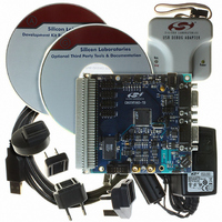
DEV KIT FOR F060/F062/F063
Manufacturer
Silicon Laboratories Inc
Type
MCUr
Datasheet
1.C8051F060-TB.pdf
(328 pages)
Specifications of C8051F060DK
Contents
Evaluation Board, Power Supply, USB Cables, Adapter and Documentation
Processor To Be Evaluated
C8051F06x
Interface Type
USB
Silicon Manufacturer
Silicon Labs
Core Architecture
8051
Silicon Core Number
C8051F060
Silicon Family Name
C8051F06x
Lead Free Status / RoHS Status
Contains lead / RoHS non-compliant
For Use With/related Products
C8051060, C8051F062 and C8051F063
Lead Free Status / Rohs Status
Lead free / RoHS Compliant
Other names
336-1214
Available stocks
Company
Part Number
Manufacturer
Quantity
Price
Company:

Part Number:
C8051F060DK
Manufacturer:
Silicon Labs
Quantity:
135


C8051F060/1/2/3/4/5/6/7
16.3. Security Options
The CIP-51 provides security options to protect the Flash memory from inadvertent modification by soft-
ware as well as prevent the viewing of proprietary program code and constants. The Program Store Write
Enable (PSCTL.0) and the Program Store Erase Enable (PSCTL.1) bits protect the Flash memory from
accidental modification by software. These bits must be explicitly set to logic 1 before software can write or
erase the Flash memory. Additional security features prevent proprietary program code and data constants
from being read or altered across the JTAG interface or by software running on the system controller.
A set of security lock bytes protect the Flash program memory from being read or altered across the JTAG
interface. Each bit in a security lock-byte protects one 8k-byte block of memory. Clearing a bit to logic 0 in
a Read Lock Byte prevents the corresponding block of Flash memory from being read across the JTAG
interface. Clearing a bit in the Write/Erase Lock Byte protects the block from JTAG erasures and/or writes.
The Scratchpad area is read or write/erase locked when all bits in the corresponding security byte are
cleared to logic 0.
On the C8051F060/1/2/3/4/5, the security lock bytes are located at 0xFBFE (Write/Erase Lock) and
0xFBFF (Read Lock), as shown in Figure 16.1. On the C8051F066/7, the security lock bytes are located at
0x7FFE (Write/Erase Lock) and 0x7FFF (Read Lock), as shown in Figure 16.2. The 512-byte sector con-
taining the lock bytes can be written to, but not erased, by software. An attempted read of a read-locked
byte returns undefined data. Debugging code in a read-locked sector is not possible through the JTAG
interface. The lock bits can always be read from and written to logic 0 regardless of the security setting
applied to the block containing the security bytes. This allows additional blocks to be protected after the
block containing the security bytes has been locked.
Important Note: To ensure protection from external access, the block containing the lock bytes
must be Write/Erase locked. On the 64 k byte devices (C8051F060/1/2/3/4/5), the page containing
the security bytes is 0xFA00-0xFBFF, and is locked by clearing bit 7 of the Write/Erase Lock Byte.
On the 32 k byte devices (C8051F066/7), the page containing the security bytes is 0x7E00-0x7FFF,
and is locked by clearing bit 3 of the Write/Erase Lock Byte. If the page containing the security
bytes is not Write/Erase locked, it is still possible to erase this page of Flash memory through the
JTAG port and reset the security bytes.
When the page containing the security bytes has been Write/Erase locked, a JTAG full device erase
must be performed to unlock any areas of Flash protected by the security bytes. A JTAG full
device erase is initiated by performing a normal JTAG erase operation on either of the security byte
locations. This operation must be initiated through the JTAG port, and cannot be performed from
firmware running on the device.
Rev. 1.2
179
Related parts for C8051F060DK
Image
Part Number
Description
Manufacturer
Datasheet
Request
R

Part Number:
Description:
SMD/C°/SINGLE-ENDED OUTPUT SILICON OSCILLATOR
Manufacturer:
Silicon Laboratories Inc
Part Number:
Description:
Manufacturer:
Silicon Laboratories Inc
Datasheet:
Part Number:
Description:
N/A N/A/SI4010 AES KEYFOB DEMO WITH LCD RX
Manufacturer:
Silicon Laboratories Inc
Datasheet:
Part Number:
Description:
N/A N/A/SI4010 SIMPLIFIED KEY FOB DEMO WITH LED RX
Manufacturer:
Silicon Laboratories Inc
Datasheet:
Part Number:
Description:
N/A/-40 TO 85 OC/EZLINK MODULE; F930/4432 HIGH BAND (REV E/B1)
Manufacturer:
Silicon Laboratories Inc
Part Number:
Description:
EZLink Module; F930/4432 Low Band (rev e/B1)
Manufacturer:
Silicon Laboratories Inc
Part Number:
Description:
I°/4460 10 DBM RADIO TEST CARD 434 MHZ
Manufacturer:
Silicon Laboratories Inc
Part Number:
Description:
I°/4461 14 DBM RADIO TEST CARD 868 MHZ
Manufacturer:
Silicon Laboratories Inc
Part Number:
Description:
I°/4463 20 DBM RFSWITCH RADIO TEST CARD 460 MHZ
Manufacturer:
Silicon Laboratories Inc
Part Number:
Description:
I°/4463 20 DBM RADIO TEST CARD 868 MHZ
Manufacturer:
Silicon Laboratories Inc
Part Number:
Description:
I°/4463 27 DBM RADIO TEST CARD 868 MHZ
Manufacturer:
Silicon Laboratories Inc
Part Number:
Description:
I°/4463 SKYWORKS 30 DBM RADIO TEST CARD 915 MHZ
Manufacturer:
Silicon Laboratories Inc
Part Number:
Description:
N/A N/A/-40 TO 85 OC/4463 RFMD 30 DBM RADIO TEST CARD 915 MHZ
Manufacturer:
Silicon Laboratories Inc
Part Number:
Description:
I°/4463 20 DBM RADIO TEST CARD 169 MHZ
Manufacturer:
Silicon Laboratories Inc