DEMO9S12XEP100 Freescale Semiconductor, DEMO9S12XEP100 Datasheet - Page 714
DEMO9S12XEP100
Manufacturer Part Number
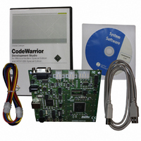
DEMO9S12XEP100
Description
BOARD DEMO FOR MC9S12XEP100
Manufacturer
Freescale Semiconductor
Type
MCUr
Datasheet
1.EVB9S12XEP100.pdf
(1328 pages)
Specifications of DEMO9S12XEP100
Contents
Board, Cables, CD
Processor To Be Evaluated
MC9S12XEP100
Data Bus Width
16 bit
Interface Type
RS-232
Silicon Manufacturer
Freescale
Core Architecture
S12
Core Sub-architecture
S12
Silicon Core Number
MC9S12
Silicon Family Name
S12XE
Rohs Compliant
Yes
For Use With/related Products
MC9S12XEP100
Lead Free Status / RoHS Status
Lead free / RoHS Compliant
Available stocks
Company
Part Number
Manufacturer
Quantity
Price
Company:

Part Number:
DEMO9S12XEP100
Manufacturer:
PANASONIC
Quantity:
46 000
Company:
Part Number:
DEMO9S12XEP100
Manufacturer:
Freescale Semiconductor
Quantity:
135


Chapter 19 Pulse-Width Modulator (S12PWM8B8CV1)
8-bit counter is re-loaded. The output signal from this circuit is further divided by two. This gives a greater
range with only a slight reduction in granularity. Clock SA equals clock A divided by two times the value
in the PWMSCLA register.
Similarly, clock B is used as an input to an 8-bit down counter followed by a divide by two producing clock
SB. Thus, clock SB equals clock B divided by two times the value in the PWMSCLB register.
As an example, consider the case in which the user writes $FF into the PWMSCLA register. Clock A for
this case will be E divided by 4. A pulse will occur at a rate of once every 255x4 E cycles. Passing this
through the divide by two circuit produces a clock signal at an E divided by 2040 rate. Similarly, a value
of $01 in the PWMSCLA register when clock A is E divided by 4 will produce a clock at an E divided by
8 rate.
Otherwise, when changing rates the counter would have to count down to $01 before counting at the proper
rate. Forcing the associated counter to re-load the scale register value every time PWMSCLA or
PWMSCLB is written prevents this.
19.4.1.3
Each PWM channel has the capability of selecting one of two clocks. For channels 0, 1, 4, and 5 the clock
choices are clock A or clock SA. For channels 2, 3, 6, and 7 the choices are clock B or clock SB. The clock
selection is done with the PCLKx control bits in the PWMCLK register.
19.4.2
The main part of the PWM module are the actual timers. Each of the timer channels has a counter, a period
register and a duty register (each are 8-bit). The waveform output period is controlled by a match between
the period register and the value in the counter. The duty is controlled by a match between the duty register
714
Writing to PWMSCLA or PWMSCLB causes the associated 8-bit down counter to be re-loaded.
Because of an order from the United States International Trade Commission, BGA-packaged product lines and partnumbers
indicated here currently are not available from Freescale for import or sale in the United States prior to September 2010
PWM Channel Timers
Clock Select
Clock SA = Clock A / (2 * PWMSCLA)
When PWMSCLA = $00, PWMSCLA value is considered a full scale value
of 256. Clock A is thus divided by 512.
Clock SB = Clock B / (2 * PWMSCLB)
When PWMSCLB = $00, PWMSCLB value is considered a full scale value
of 256. Clock B is thus divided by 512.
Writing to the scale registers while channels are operating can cause
irregularities in the PWM outputs.
Changing clock control bits while channels are operating can cause
irregularities in the PWM outputs.
MC9S12XE-Family Reference Manual , Rev. 1.23
NOTE
NOTE
NOTE
NOTE
Freescale Semiconductor
Related parts for DEMO9S12XEP100
Image
Part Number
Description
Manufacturer
Datasheet
Request
R

Part Number:
Description:
Manufacturer:
Freescale Semiconductor, Inc
Datasheet:
Part Number:
Description:
Manufacturer:
Freescale Semiconductor, Inc
Datasheet:
Part Number:
Description:
Manufacturer:
Freescale Semiconductor, Inc
Datasheet:
Part Number:
Description:
Manufacturer:
Freescale Semiconductor, Inc
Datasheet:
Part Number:
Description:
Manufacturer:
Freescale Semiconductor, Inc
Datasheet:
Part Number:
Description:
Manufacturer:
Freescale Semiconductor, Inc
Datasheet:
Part Number:
Description:
Manufacturer:
Freescale Semiconductor, Inc
Datasheet:
Part Number:
Description:
Manufacturer:
Freescale Semiconductor, Inc
Datasheet:
Part Number:
Description:
Manufacturer:
Freescale Semiconductor, Inc
Datasheet:
Part Number:
Description:
Manufacturer:
Freescale Semiconductor, Inc
Datasheet:
Part Number:
Description:
Manufacturer:
Freescale Semiconductor, Inc
Datasheet:
Part Number:
Description:
Manufacturer:
Freescale Semiconductor, Inc
Datasheet:
Part Number:
Description:
Manufacturer:
Freescale Semiconductor, Inc
Datasheet:
Part Number:
Description:
Manufacturer:
Freescale Semiconductor, Inc
Datasheet:
Part Number:
Description:
Manufacturer:
Freescale Semiconductor, Inc
Datasheet: