DEMO9S12XEP100 Freescale Semiconductor, DEMO9S12XEP100 Datasheet - Page 155
DEMO9S12XEP100
Manufacturer Part Number
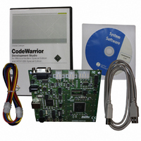
DEMO9S12XEP100
Description
BOARD DEMO FOR MC9S12XEP100
Manufacturer
Freescale Semiconductor
Type
MCUr
Datasheet
1.EVB9S12XEP100.pdf
(1328 pages)
Specifications of DEMO9S12XEP100
Contents
Board, Cables, CD
Processor To Be Evaluated
MC9S12XEP100
Data Bus Width
16 bit
Interface Type
RS-232
Silicon Manufacturer
Freescale
Core Architecture
S12
Core Sub-architecture
S12
Silicon Core Number
MC9S12
Silicon Family Name
S12XE
Rohs Compliant
Yes
For Use With/related Products
MC9S12XEP100
Lead Free Status / RoHS Status
Lead free / RoHS Compliant
Available stocks
Company
Part Number
Manufacturer
Quantity
Price
Company:

Part Number:
DEMO9S12XEP100
Manufacturer:
PANASONIC
Quantity:
46 000
Company:
Part Number:
DEMO9S12XEP100
Manufacturer:
Freescale Semiconductor
Quantity:
135


1. Read: Anytime.
Freescale Semiconductor
Write: Anytime.
DDRJ
DDRJ
DDRJ
DDRJ
DDRJ
DDRJ
Field
7
6
5
4
3
2
Port J data direction—
This register controls the data direction of pin 7.
The enabled CAN4 or routed CAN0 forces the I/O state to be an output. The enabled IIC0 module forces this pin to
be a open drain output. In those cases the data direction bits will not change. The DDRM bits revert to controlling
the I/O direction of a pin when the associated peripheral module is disabled.
1 Associated pin is configured as output.
0 Associated pin is configured as input.
Port J data direction—
This register controls the data direction of pin 6.
The enabled CAN4 or routed CAN0 forces the I/O state to be an input. The enabled IIC0 module forces this pin to
be a open drain output. In those cases the data direction bits will not change. The DDRM bits revert to controlling
the I/O direction of a pin when the associated peripheral module is disabled.
1 Associated pin is configured as output.
0 Associated pin is configured as input.
Port J data direction—
This register controls the data direction of pin 5.
The enabled CS2 signal forces the I/O state to be an output. The enabled IIC1 module forces this pin to be a open
drain output. In those cases the data direction bits will not change. The DDRM bits revert to controlling the I/O
direction of a pin when the associated peripheral module is disabled.
1 Associated pin is configured as output.
0 Associated pin is configured as input.
Port J data direction—
This register controls the data direction of pin 4.
The enabled CS0 signal forces the I/O state to be an output. The enabled IIC1 module forces this pin to be a open
drain output. In those cases the data direction bits will not change. The DDRM bits revert to controlling the I/O
direction of a pin when the associated peripheral module is disabled.
1 Associated pin is configured as output.
0 Associated pin is configured as input.
Port J data direction—
This register controls the data direction of pin 3.
1 Associated pin is configured as output.
0 Associated pin is configured as input.
Port J data direction—
This register controls the data direction of pin 2.
The enabled CS1 signal forces the I/O state to be an output. In those cases the data direction bits will not change.
The DDRM bits revert to controlling the I/O direction of a pin when the associated peripheral module is disabled.
1 Associated pin is configured as output.
0 Associated pin is configured as input.
Table 2-59. DDRJ Register Field Descriptions
MC9S12XE-Family Reference Manual , Rev. 1.23
Description
Chapter 2 Port Integration Module (S12XEPIMV1)
155
Related parts for DEMO9S12XEP100
Image
Part Number
Description
Manufacturer
Datasheet
Request
R

Part Number:
Description:
Manufacturer:
Freescale Semiconductor, Inc
Datasheet:
Part Number:
Description:
Manufacturer:
Freescale Semiconductor, Inc
Datasheet:
Part Number:
Description:
Manufacturer:
Freescale Semiconductor, Inc
Datasheet:
Part Number:
Description:
Manufacturer:
Freescale Semiconductor, Inc
Datasheet:
Part Number:
Description:
Manufacturer:
Freescale Semiconductor, Inc
Datasheet:
Part Number:
Description:
Manufacturer:
Freescale Semiconductor, Inc
Datasheet:
Part Number:
Description:
Manufacturer:
Freescale Semiconductor, Inc
Datasheet:
Part Number:
Description:
Manufacturer:
Freescale Semiconductor, Inc
Datasheet:
Part Number:
Description:
Manufacturer:
Freescale Semiconductor, Inc
Datasheet:
Part Number:
Description:
Manufacturer:
Freescale Semiconductor, Inc
Datasheet:
Part Number:
Description:
Manufacturer:
Freescale Semiconductor, Inc
Datasheet:
Part Number:
Description:
Manufacturer:
Freescale Semiconductor, Inc
Datasheet:
Part Number:
Description:
Manufacturer:
Freescale Semiconductor, Inc
Datasheet:
Part Number:
Description:
Manufacturer:
Freescale Semiconductor, Inc
Datasheet:
Part Number:
Description:
Manufacturer:
Freescale Semiconductor, Inc
Datasheet: