DK-DEV-3SL150N Altera, DK-DEV-3SL150N Datasheet - Page 29
DK-DEV-3SL150N
Manufacturer Part Number
DK-DEV-3SL150N
Description
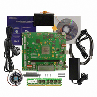
KIT DEVELOPMENT STRATIX III
Manufacturer
Altera
Series
Stratix® IIIr
Type
FPGAr
Datasheets
1.EP3SL150F780C4N.pdf
(16 pages)
2.EP3SL150F780C4N.pdf
(332 pages)
3.DK-DEV-3SL150N.pdf
(34 pages)
Specifications of DK-DEV-3SL150N
Contents
Development Platform, Cables and Software
Silicon Manufacturer
Altera
Core Architecture
FPGA
Core Sub-architecture
Stratix
Silicon Core Number
EP3S
Silicon Family Name
Stratix III
Kit Contents
Development Board, Cable And Accessories
Rohs Compliant
Yes
For Use With/related Products
EP3SL150F152
Lead Free Status / RoHS Status
Lead free / RoHS Compliant
Other names
544-2568
Available stocks
Company
Part Number
Manufacturer
Quantity
Price
Company:

Part Number:
DK-DEV-3SL150N
Manufacturer:
Altera
Quantity:
135


Appendix A: Programming the Flash Device
Parallel Flash Loader Instantiation
Parallel Flash Loader Instantiation
Programming the Flash Device
© August 2008 Altera Corporation
f
6. Click Generate. Generation takes a short time and it is confirmed by a
You now have a successfully generated .pof that can be programmed to the flash
device to automatically configure the FPGA on your Stratix III development board.
The development kit includes a PFL megafunction design, stratixIII_3sl150_dev_pfl,
in the directory <path>\examples. The Quartus II software uses the PFL to write
programming files to the flash device, which then loads the FPGA on power up.
To write to a flash device, you must first program the PFL into the FPGA by using the
Quartus II software as described in
steps
For more information about the PFL megafunction, refer to
Flash Loader with the Quartus II
To program the flash device on the development board, you must first create a .pof
flash file as described in
procedure describes programming the PFL into the FPGA, then uses the PFL to write
the .pof flash file into the flash device.
To download a configuration bit stream into the flash device, perform the following
steps:
1. Ensure that the POWER switch SW4 is in the OFF (or DOWN) position.
2. Verify the switch SW1 and jumper settings shown in
3. Connect the USB cable to the USB port on the board.
4. Cycle the POWER switch OFF then ON.
5. On the Tools menu in the Quartus II software, click Programmer.
6. Click Add File and select
7. Turn on the Program/Configure option for the added file.
8. Click Start to download the selected configuration file to FPGA
“Generated… pof successfully” message.
<path>\examples\stratixIII_3sl150_dev_pfl\stratixIII_3sl150_dev_pfl.sof.
FPGA is configured when the progress bar reaches 100%, after which it is ready to
access and program the flash device.
1
through 8.
“Creating a Flash File” on page
Software.
“Programming the Flash Device” on page
Table 4–2 on page
A–1. The following
Stratix III Development Kit User Guide
AN 386: Using the Parallel
(Figure
4–3.
A–2). The
A–3,
A–3
Related parts for DK-DEV-3SL150N
Image
Part Number
Description
Manufacturer
Datasheet
Request
R

Part Number:
Description:
KIT DEV ARRIA II GX FPGA 2AGX125
Manufacturer:
Altera
Datasheet:

Part Number:
Description:
KIT DEV CYCLONE III LS EP3CLS200
Manufacturer:
Altera
Datasheet:

Part Number:
Description:
KIT DEV STRATIX IV FPGA 4SE530
Manufacturer:
Altera
Datasheet:

Part Number:
Description:
KIT DEV FPGA 2AGX260 W/6.375G TX
Manufacturer:
Altera
Datasheet:

Part Number:
Description:
KIT DEV MAX V 5M570Z
Manufacturer:
Altera
Datasheet:

Part Number:
Description:
KIT DEV STRATIX V FPGA 5SGXEA7
Manufacturer:
Altera
Datasheet:

Part Number:
Description:
KIT DEVELOPMENT STRATIX IV
Manufacturer:
Altera
Datasheet:

Part Number:
Description:
KIT DEV ARRIA GX 1AGX60N
Manufacturer:
Altera
Datasheet:
Part Number:
Description:
KIT STARTER CYCLONE IV GX
Manufacturer:
Altera
Datasheet:
Part Number:
Description:
KIT DEVELOPMENT STRATIX IV
Manufacturer:
Altera
Datasheet:

Part Number:
Description:
CPLD, EP610 Family, ECMOS Process, 300 Gates, 16 Macro Cells, 16 Reg., 16 User I/Os, 5V Supply, 35 Speed Grade, 24DIP
Manufacturer:
Altera Corporation
Datasheet:
Part Number:
Description:
CPLD, EP610 Family, ECMOS Process, 300 Gates, 16 Macro Cells, 16 Reg., 16 User I/Os, 5V Supply, 15 Speed Grade, 24DIP
Manufacturer:
Altera Corporation
Datasheet: