DK-DEV-3SL150N Altera, DK-DEV-3SL150N Datasheet - Page 16
DK-DEV-3SL150N
Manufacturer Part Number
DK-DEV-3SL150N
Description
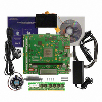
KIT DEVELOPMENT STRATIX III
Manufacturer
Altera
Series
Stratix® IIIr
Type
FPGAr
Datasheets
1.EP3SL150F780C4N.pdf
(16 pages)
2.EP3SL150F780C4N.pdf
(332 pages)
3.DK-DEV-3SL150N.pdf
(34 pages)
Specifications of DK-DEV-3SL150N
Contents
Development Platform, Cables and Software
Silicon Manufacturer
Altera
Core Architecture
FPGA
Core Sub-architecture
Stratix
Silicon Core Number
EP3S
Silicon Family Name
Stratix III
Kit Contents
Development Board, Cable And Accessories
Rohs Compliant
Yes
For Use With/related Products
EP3SL150F152
Lead Free Status / RoHS Status
Lead free / RoHS Compliant
Other names
544-2568
Available stocks
Company
Part Number
Manufacturer
Quantity
Price
Company:

Part Number:
DK-DEV-3SL150N
Manufacturer:
Altera
Quantity:
135


4–2
Figure 4–1. Stratix III Development Board Layout and Components
Stratix III Development Kit User Guide
Power Display (U27)
Present LED (D17)
HSMC Port A (J18)
HSMC Port B (J8)
Present LED (D10)
TX/RX Activity LEDs
User DIP Switch (SW5)
MSEL0 to GND
LEDs (D11, D12)
HSMC Port A
Jumper (J13)
HSMC Port B
TX/RX Activity
HSMC Port A
HSMC Port B
(D2, D3)
Speaker Header (J1)
Before powering up, prepare the board as follows:
1. If cards are plugged into the HSMC ports, remove them.
2. Ensure that the POWER switch SW4 is in the OFF (or DOWN) position.
3. Configure the 8-position SW2 DIP switch to the default settings in
Table 4–1. Switch SW2 Settings (Part 1 of 2)
(Behind the LCD Screen)
Switch
QDRII+ SRAM (U15)
1
2
3
4
User Push Buttons
(S2 through S5)
mW/mA
V/W
RSV0
RSV1
Rotary Switch (SW6)
Flash Memory Device (U9)
Power Select
Name
24 MHz Crystal (Y4)
DDR2 SDRAM
DIMM Connector (J19)
Position 0
Done LED (D32)
JTAG Control DIP Switch (SW1)
CPLD (U5)
FPGA (U22)
Push Button (S6)
Stratix III
Configuration
MAX II
mW
V
CPU Reset
MAX_RESERVE0
MAX_RESERVE1
Function
125 MHz MAX II Clock (Y1)
Device Select (J2)
LEDs (D33-D36)
Board-Specific
Jumper
Position 1
mA
24 MHz Crystal (Y2)
Chapter 4: Development Board Setup
W
User LEDs
(D20 through D27)
Type B USB
Connector (J5)
Reset Configuration
Push Button (S7)
© August 2008 Altera Corporation
Clock In/Out SMAs (J16, J17)
DDR2 SDRAM
(U17, U20)
Ethernet PHY TX/RX
Activity LEDs (D14, D15)
Power LED (D16)
6 MHz
Crystal (Y3)
MAX II Control
DIP Switch (SW2)
Factory Configuration
Push Button (S1)
User Display (U28)
PGM Config Select
Rotary Switch (SW3)
Power Switch (SW4)
Ethernet PHY
LEDs (D6, D7, D8) and
Duplex LED (D9)
DC Power Jack (J21)
RJ-45 Ethernet
Connector (J14)
Powering Up the Board
Table
Position
Default
4–1.
0
1
X
X
Related parts for DK-DEV-3SL150N
Image
Part Number
Description
Manufacturer
Datasheet
Request
R

Part Number:
Description:
KIT DEV ARRIA II GX FPGA 2AGX125
Manufacturer:
Altera
Datasheet:

Part Number:
Description:
KIT DEV CYCLONE III LS EP3CLS200
Manufacturer:
Altera
Datasheet:

Part Number:
Description:
KIT DEV STRATIX IV FPGA 4SE530
Manufacturer:
Altera
Datasheet:

Part Number:
Description:
KIT DEV FPGA 2AGX260 W/6.375G TX
Manufacturer:
Altera
Datasheet:

Part Number:
Description:
KIT DEV MAX V 5M570Z
Manufacturer:
Altera
Datasheet:

Part Number:
Description:
KIT DEV STRATIX V FPGA 5SGXEA7
Manufacturer:
Altera
Datasheet:

Part Number:
Description:
KIT DEVELOPMENT STRATIX IV
Manufacturer:
Altera
Datasheet:

Part Number:
Description:
KIT DEV ARRIA GX 1AGX60N
Manufacturer:
Altera
Datasheet:
Part Number:
Description:
KIT STARTER CYCLONE IV GX
Manufacturer:
Altera
Datasheet:
Part Number:
Description:
KIT DEVELOPMENT STRATIX IV
Manufacturer:
Altera
Datasheet:

Part Number:
Description:
CPLD, EP610 Family, ECMOS Process, 300 Gates, 16 Macro Cells, 16 Reg., 16 User I/Os, 5V Supply, 35 Speed Grade, 24DIP
Manufacturer:
Altera Corporation
Datasheet:
Part Number:
Description:
CPLD, EP610 Family, ECMOS Process, 300 Gates, 16 Macro Cells, 16 Reg., 16 User I/Os, 5V Supply, 15 Speed Grade, 24DIP
Manufacturer:
Altera Corporation
Datasheet: