RDK-138 Power Integrations, RDK-138 Datasheet - Page 7
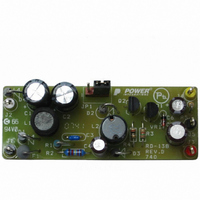
RDK-138
Manufacturer Part Number
RDK-138
Description
KIT REF DESIGN 1.2W PS TN FAMILY
Manufacturer
Power Integrations
Specifications of RDK-138
Mfg Application Notes
LinkSwitch-TN Design Guide, AN-37
Main Purpose
AC/DC, Non-Isolated
Outputs And Type
2, Non-Isolated
Power - Output
1.2W
Voltage - Output
12V, 5V
Current - Output
80mA, 50mA
Voltage - Input
85 ~ 265VAC
Regulator Topology
Buck
Frequency - Switching
66kHz
Board Type
Fully Populated
Utilized Ic / Part
LNK304
Product
Accessories & Kits
Lead Free Status / RoHS Status
Not applicable / Not applicable
Other names
596-1197


12-Nov-2007
RDR-138 1.2 W Non Isolated Dual Output Supply
4.3 Output Rectification and Filtering
During U1’s conduction time, current through inductor L2 linearly ramps up, delivering
energy to the load and to capacitor C5. During U1’s on time, the energy from the
inductor is also used by the linear regulator circuitry.
During U1’s off time, the voltage across inductor L2 changes its polarity in an attempt to
maintain current flow and thus forward biases freewheeling diode D2.
During D2’s
conduction time, the energy stored in the inductor is delivered to capacitor C5, the load,
and the linear regulator while the current through the inductor ramps downward.
Freewheeling diode D2 provides output rectification and should be an ultrafast type
diode, such as UF4005 with a reverse recovery time t
≤75 ns (In this case the BYV26C
rr
was used to improve efficiency). This is a sufficient reverse recovery time as this design
operates in the mostly discontinuous operating mode (MDCM). Slower diodes result in
large leading edge current spikes, which will result in prematurely terminated switching
cycles due to exceeding the device’s internal current limit. This diode should also be able
to withstand the maximum DC bus voltage plus an appropriate margin (usually at least
25%).
4.4 Feedback Network
As previously mentioned, the LinkSwitch-TN family of devices uses a simple and efficient
On/Off control scheme.
The on time of the MOSFET is determined by the output
inductor’s value, the current limit of the device and the value of the DC bus voltage. This
is due to the use of the On/Off control scheme, which turns off the device once the
current limit is reached.
The device will therefore reach its internal current limit during every enabled switching
cycle. Thus the output voltage is regulated by disabling (skipping) switching cycles.
Switching cycles are skipped whenever current in excess of 49 µA is delivered into the
feedback (FB) pin.
A feedback signal is derived from the output (the voltage across C5) through a simple
voltage divider formed by 1 % tolerance metal film resistors R1 and R2. The input signal
to this voltage divider is the voltage on capacitor C4, which closely tracks the output
voltage and is charged whenever diode D3 is forward biased.
Diode D3 is necessary to prevent the FB pin from delivering current to the output
whenever the MOSFET is conducting, since the FB pin has a voltage of 1.65 V +
V
. The voltage divider does not need to take into account D3’s forward voltage
SOURCE
drop because, to a first order, D2 and D3’s forward voltages are equal, and thus the
feedback network tracks the output voltage.
Power Integrations
Tel: +1 408 414 9200 Fax: +1 408 414 9201
Page 7 of 28
www.powerint.com
Related parts for RDK-138
Image
Part Number
Description
Manufacturer
Datasheet
Request
R

Part Number:
Description:
KIT REF DESIGN FOR LNK457D
Manufacturer:
Power Integrations
Datasheet:

Part Number:
Description:
REFERENCE DESIGN LINKSWITCH-PH
Manufacturer:
Power Integrations
Datasheet:

Part Number:
Description:
KIT REF DESIGN FOR LNK403EG
Manufacturer:
Power Integrations
Datasheet:

Part Number:
Description:
KIT REF DESIGN FOR LNK406EG
Manufacturer:
Power Integrations
Datasheet:

Part Number:
Description:
KIT REF DESIGN LINKSWITCH-CV
Manufacturer:
Power Integrations
Datasheet:

Part Number:
Description:
KIT REF DESIGN LINKSWITCH 2
Manufacturer:
Power Integrations
Datasheet:

Part Number:
Description:
Specifications: Family: Eval Boards - DC/DC & AC/DC (Off-Line) SMPS ; Series: HiperLCS™ ; Main Purpose: DC/DC, Step Down ; Outputs and Type: 1, Isolated ; Power - Output: 150W ; Voltage - Output: 24V ; Current - Output: 6.25A ; Voltage - Input:
Manufacturer:
Power Integrations, Inc.
Datasheet:

Part Number:
Description:
KIT DESIGN REF TINYSWITCH-III
Manufacturer:
Power Integrations
Datasheet:

Part Number:
Description:
KIT DESIGN REF LINKSWITCH LP
Manufacturer:
Power Integrations
Datasheet:

Part Number:
Description:
KIT REF DESIGN LED LINKSWITCH TN
Manufacturer:
Power Integrations
Datasheet:
Part Number:
Description:
KIT REF DESIGN PG LINKSWITCH-II
Manufacturer:
Power Integrations
Datasheet:
Part Number:
Description:
REFERENCE DESIGN LINKSWITCH-PL
Manufacturer:
Power Integrations
Datasheet:
Part Number:
Description:
REFERENCE DESIGN LINKSWITCH-PH
Manufacturer:
Power Integrations
Datasheet:

Part Number:
Description:
KIT REF DESIGN 36-72W MOTOR DRVR
Manufacturer:
Power Integrations
Datasheet:
Part Number:
Description:
Specifications: Manufacturer: Power Integrations ; Output Voltage: 380 VDC ; Input / Supply Voltage (Max): 264 VAC ; Input / Supply Voltage (Min): 90 VAC ; Mounting Style: Through Hole ; Output Current: 0.913 A ; Output Power: 347 W
Manufacturer:
Power Integrations, Inc.