RDK-138 Power Integrations, RDK-138 Datasheet - Page 6
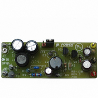
RDK-138
Manufacturer Part Number
RDK-138
Description
KIT REF DESIGN 1.2W PS TN FAMILY
Manufacturer
Power Integrations
Specifications of RDK-138
Mfg Application Notes
LinkSwitch-TN Design Guide, AN-37
Main Purpose
AC/DC, Non-Isolated
Outputs And Type
2, Non-Isolated
Power - Output
1.2W
Voltage - Output
12V, 5V
Current - Output
80mA, 50mA
Voltage - Input
85 ~ 265VAC
Regulator Topology
Buck
Frequency - Switching
66kHz
Board Type
Fully Populated
Utilized Ic / Part
LNK304
Product
Accessories & Kits
Lead Free Status / RoHS Status
Not applicable / Not applicable
Other names
596-1197


4 Circuit Description
The power supply described has a jumper that allows for the supply to operate using
either the buck topology–enabling the two outputs to be configured as positive outputs
with respect to AC neutral–or a buck-derived topology–enabling one of the two outputs to
be configured as a negative output with respect to AC neutral. Shorting pins 1 and 2 of
JP1 will operate the supply in a buck-derived topology, while shorting pins 2 and 3 will
operate the supply in the buck topology. See Figure 1 for an illustration of the two jumper
positions.
While in the buck topology, the power supply has a 12 V output capable of delivering 80
mA and a 5 V output capable of 50 mA. If the supply is in the buck-derived topology, it
provides a –5 V output when referenced to return and can provide 50 mA of current. The
other output can be used to supply 80 mA and a 7 V output when referenced to return, or
it can be configured as a floating12 V output.
The data presented in the report were taken using the buck topology with both outputs
configured as positive outputs.
4.1 AC Input Rectification and EMI Filtering
The AC input is half-wave rectified by fast recovery diode D1 and general purpose diode
D4. The fast recovery diode helps to improve differential mode conducted EMI. A second
diode, D4, is placed in the return conductor of the supply to provide EMI noise gating.
This helps minimize common mode noise and reduce EMI.
Included in the path of the AC input is a fusible flameproof resistor, RF1. In the event of
a catastrophic failure, the failure mechanism of this resistor is open circuit, with no flame
or smoke emitted. Additionally, this resistor is wire wound to prevent premature failure
due to the inrush currents when AC is applied.
The input stage is completed by capacitors C1 and C2, which provide bulk energy
storage. Inductor L1 forms a π-filter with the bulk capacitors, which helps to minimize
differential mode conducted EMI.
4.2 LinkSwitch-TN Device
LinkSwitch-TN is a low-cost, full-featured monolithic IC integrating both the control
circuitry and high voltage MOSFET switch into the same device. Some of the most
prominent features of the device include an On/Off type controller, a maximum switching
frequency of 66 kHz, which includes ±4 kHz of frequency jitter to help reduce EMI and a
700 V MOSFET. The LinkSwitch-TN device also includes a number of protection
features, including output short-circuit protection, open loop fault protection, MOSFET
current limit protection and thermal shutdown with hysteresis. The device is powered
from the drain pin with local supply decoupling provided by the 100 nF capacitor C3
connected to the bypass pin (BP) of the LinkSwitch-TN device, U1.
Power Integrations
Tel: +1 408 414 9200 Fax: +1 408 414 9201
www.powerint.com
Page 6 of 28
Related parts for RDK-138
Image
Part Number
Description
Manufacturer
Datasheet
Request
R

Part Number:
Description:
KIT REF DESIGN FOR LNK457D
Manufacturer:
Power Integrations
Datasheet:

Part Number:
Description:
REFERENCE DESIGN LINKSWITCH-PH
Manufacturer:
Power Integrations
Datasheet:

Part Number:
Description:
KIT REF DESIGN FOR LNK403EG
Manufacturer:
Power Integrations
Datasheet:

Part Number:
Description:
KIT REF DESIGN FOR LNK406EG
Manufacturer:
Power Integrations
Datasheet:

Part Number:
Description:
KIT REF DESIGN LINKSWITCH-CV
Manufacturer:
Power Integrations
Datasheet:

Part Number:
Description:
KIT REF DESIGN LINKSWITCH 2
Manufacturer:
Power Integrations
Datasheet:

Part Number:
Description:
Specifications: Family: Eval Boards - DC/DC & AC/DC (Off-Line) SMPS ; Series: HiperLCS™ ; Main Purpose: DC/DC, Step Down ; Outputs and Type: 1, Isolated ; Power - Output: 150W ; Voltage - Output: 24V ; Current - Output: 6.25A ; Voltage - Input:
Manufacturer:
Power Integrations, Inc.
Datasheet:

Part Number:
Description:
KIT DESIGN REF TINYSWITCH-III
Manufacturer:
Power Integrations
Datasheet:

Part Number:
Description:
KIT DESIGN REF LINKSWITCH LP
Manufacturer:
Power Integrations
Datasheet:

Part Number:
Description:
KIT REF DESIGN LED LINKSWITCH TN
Manufacturer:
Power Integrations
Datasheet:
Part Number:
Description:
KIT REF DESIGN PG LINKSWITCH-II
Manufacturer:
Power Integrations
Datasheet:
Part Number:
Description:
REFERENCE DESIGN LINKSWITCH-PL
Manufacturer:
Power Integrations
Datasheet:
Part Number:
Description:
REFERENCE DESIGN LINKSWITCH-PH
Manufacturer:
Power Integrations
Datasheet:

Part Number:
Description:
KIT REF DESIGN 36-72W MOTOR DRVR
Manufacturer:
Power Integrations
Datasheet:
Part Number:
Description:
Specifications: Manufacturer: Power Integrations ; Output Voltage: 380 VDC ; Input / Supply Voltage (Max): 264 VAC ; Input / Supply Voltage (Min): 90 VAC ; Mounting Style: Through Hole ; Output Current: 0.913 A ; Output Power: 347 W
Manufacturer:
Power Integrations, Inc.