EVAL-AD7725CBZ Analog Devices Inc, EVAL-AD7725CBZ Datasheet - Page 5
EVAL-AD7725CBZ
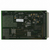
Manufacturer Part Number
EVAL-AD7725CBZ
Description
BOARD EVALUATION FOR AD7725
Manufacturer
Analog Devices Inc
Datasheet
1.AD7725BSZ.pdf
(28 pages)
Specifications of EVAL-AD7725CBZ
Number Of Adc's
1
Number Of Bits
16
Sampling Rate (per Second)
900k
Data Interface
Serial, Parallel
Inputs Per Adc
1 Differential
Input Range
±VREF
Power (typ) @ Conditions
615mW @ 900kSPS
Voltage Supply Source
Analog and Digital
Operating Temperature
-40°C ~ 85°C
Utilized Ic / Part
AD7725
Lead Free Status / RoHS Status
Lead free / RoHS Compliant


TIMING SPECIFICATIONS
Parameter
CLKIN Frequency
CLKIN Period (t
CLKIN Low Pulse Width
CLKIN High Pulse Width
CLKIN Rise Time
CLKIN Fall Time
CLKIN to SCO Delay
SCO Period:
SERIAL INTERFACE (DSP MODE ONLY)
SERIAL INTERFACE (DSP AND BFR MODES)
SERIAL INTERFACE (EPROM MODE)
PARALLEL INTERFACE
NOTES
1
2
3
REV. A
Guaranteed by design.
Guaranteed by characterization. All input signals are specified with tr
Measured with the load circuit in Figure 2 and defined as the time required for the output to cross 0.8 V and 2.4 V.
FSI Setup Time before SCO Transition
FSI Hold Time after SCO Transition
SDI Setup Time
SDI Hold Time
SCO Transition to FSO High Delay
SCO Transition to FSO Low Delay
SDO Setup before SCO Transition
SDO Hold after SCO Transition
SCO High Time
SCO Low Time
SOE Low to First SCO Rising Edge
Data Setup before SCO Rising Edge
DATA WRITE
DATA READ
STATUS READ/INSTRUCTION WRITE
RS Low to CS Low
WR Setup before CS Low
RS Hold after CS Rising Edge
CS Pulse Width
WR Hold after CS Rising Edge
Data Setup Time
Data Hold Time
RS Low to CS Low
RD Setup before CS Low
RS Hold after CS Rising Edge
RD Hold after CS Rising Edge
Data Valid after CS Falling Edge
Data Hold after CS Rising Edge
CS Duty Cycle
Interrupt Clear after CS Low
RD Setup to CS Low
RD Hold after CS Rising Edge
Read Data Access Time
Read Data Hold after CS Rising Edge
Write Data Setup before CS Rising Edge
Write Data Hold after CS Rising Edge
CLK
SCR = 0
SCR = 1
= 1/f
CLKIN
3
)
1, 2
3
(AVDD = 5 V
unless otherwise noted.)
Symbol
f
t
t
t
t
t
t
t
t
t
t
t
t
t
t
t
t
t
t
t
t
t
t
t
t
t
t
t
t
t
t
t
t
t
t
t
t
t
t
t
t
t
5%; DV
CLKIN
1
2
3
4
5
6
7
7
8
9
10
11
12
13
14
15
16
17
18
19
20
21
22
23
24
25
26
27
28
29
30
31
32
33
34
35
36
37
38
39
40
tf
5 ns (10% to 90% of DV
DD
–5–
= 5 V
Min
1
0.07
0.45
0.45
5
5
30
0
30
0
0
15
15
0
50
0
10
5
15
15
0
0
10
1
15
10
10
5
5%; AGND = DGND = 0 V, REF2 = 2.5 V,
t
t
1
1
DD
) and timed from a voltage level of 1.6 V.
35
1
2
22
Typ
Max
14.4
1
0.55
0.55
50
20
20
10
8
8
20
30
15
0
30
t
t
1
1
Unit
MHz
µs
ns
ns
ns
t
t
ns
ns
ns
ns
ns
ns
ns
ns
t
t
t
ns
ns
ns
ns
ns
ns
ns
ns
ns
ns
ns
ns
ns
ns
t
ns
ns
ns
ns
ns
ns
ns
CLK
CLK
CLK
CLK
CLK
CLK
AD7725
Related parts for EVAL-AD7725CBZ
Image
Part Number
Description
Manufacturer
Datasheet
Request
R


Part Number:
Description:
BOARD EVAL FOR SI270X-A
Manufacturer:
Silicon Laboratories Inc
Datasheet:

Part Number:
Description:
BUCK CONV REF DESIGN KIT IP1201
Manufacturer:
International Rectifier
Datasheet:
Part Number:
Description:
BOARD DEMO SYNC DUAL BUCK CNVTER
Manufacturer:
International Rectifier
Datasheet:
Part Number:
Description:
BOARD DEMO SYNC BUCK CONVETER
Manufacturer:
International Rectifier
Datasheet:

Part Number:
Description:
EVALBOARD/EB Omnidirectional microphone - Analog
Manufacturer:
Analog Devices
Datasheet:
Part Number:
Description:
EVALBOARD/EB Omnidirectional microphone - Analog
Manufacturer:
Analog Devices
Datasheet:


Part Number:
Description:
BOARD EVAL LED DRIVER LT3756
Manufacturer:
Linear Technology
Datasheet:

Part Number:
Description:
BOARD EVAL FOR AD7741/7742
Manufacturer:
Analog Devices Inc
Datasheet:

Part Number:
Description:
±1.7g Dual-Axis IMEMS Accelerometer Evaluation Board
Manufacturer:
Analog Devices Inc
Datasheet:

Part Number:
Description:
IC MULTIPLIER ANALOG 8-SOIC T/R
Manufacturer:
Analog Devices Inc
Datasheet:

Part Number:
Description:
IC ANALOG MULTIPLIER 8-DIP
Manufacturer:
Analog Devices Inc
Datasheet:
Part Number:
Description:
IC ANALOG MULTIPLIER 8-SOIC
Manufacturer:
Analog Devices Inc
Datasheet:
Part Number:
Description:
IC ANALOG MULTIPLIER 8-DIP
Manufacturer:
Analog Devices Inc
Datasheet: