EVAL-AD7725CBZ Analog Devices Inc, EVAL-AD7725CBZ Datasheet
EVAL-AD7725CBZ
Specifications of EVAL-AD7725CBZ


Related parts for EVAL-AD7725CBZ


EVAL-AD7725CBZ Summary of contents
Page 1
... Filter Wizard allows the user to design different filter types and generates the appropriate configuration file to be down- loaded to the postprocessor. The AD7725 also has an internal default filter for evaluation purposes. It provides 16-bit performance for input bandwidths up to 350 kHz with an output word rate of 900 kHz maximum. The input sample rate is set either by the crystal oscillator or an external clock ...
Page 2
AD7725–SPECIFICATIONS Parameter DYNAMIC SPECIFICATIONS Bipolar Mode 3 Signal-to-Noise 3, 5 Total Harmonic Distortion 3, 5 Spurious Free Dynamic Range Unipolar Mode 3 Signal-to-Noise 3, 5 Total Harmonic Distortion ANALOG INPUTS Full-Scale Input Span Bipolar Mode Unipolar Mode Absolute Input Voltage ...
Page 3
Parameter ALL LOGIC INPUTS I , Input Current Input Capacitance IN LOGIC OUTPUTS V , Output High Voltage Output Low Voltage OL 10 POWER SUPPLIES ...
Page 4
AD7725 Preset Filter, Default Filter, and Postprocessor Characteristics Parameter Test Conditions/Comments DIGITAL FILTER RESPONSE PRESET FIR Data Output Rate Stop-Band Attenuation Low-Pass Corner Frequency 3 Group Delay 3 Settling Time DEFAULT FILTER Internal FIR Filter Stored in ROM Number of ...
Page 5
TIMING SPECIFICATIONS Parameter CLKIN Frequency CLKIN Period (t = 1/f ) CLK CLKIN CLKIN Low Pulse Width CLKIN High Pulse Width CLKIN Rise Time CLKIN Fall Time CLKIN to SCO Delay SCO Period: SCR = 0 SCR = ...
Page 6
AD7725 Figure 2. Load Circuit for Digital Output Timing Specifications t 5 2.3V CLKIN 0. SCO SCR = SCO SCR = 1 SCO CFMT = FSI SDI FSO SDO ...
Page 7
INT RD/ DB0 DB15 – Figure 6. Parallel Mode (Writing Data to the AD7725) INT RD/ DB0 DB15 – Figure 7. Parallel Mode (Reading Data from the AD7725) REV SCO ...
Page 8
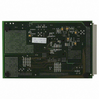
... BRD2 NOTES Metric Quad Flat Package (MQFP). 2 This board can be used as a standalone evaluation board or in conjunction with the Evaluation Board Controller for evaluation/demonstration purposes accom- panied by software and technical documentation. 3 Evaluation Board Controller. This board is a complete unit allowing control and communicate with all Analog Devices boards ending in the CB designator ...
Page 9
EFMT/DB2 ERR/DB1 SDI/DB0 CFMT/RS DVAL/INT Pin No. Mnemonic S/P Description 1 EFMT/DB2 Serial Mode. EFMT–Serial Clock Format, Logic Input. This clock format pin selects the clock edge to be used during configuration. When EFMT is low, Serial Data In is ...
Page 10
AD7725 Pin No. Mnemonic S/P Description DVAL/INT Serial Mode. DVAL–Data Valid Logic Output. This output is low when there are no 5 overflows in the postprocessor and goes high when an overflow occurs in the postprocessor. Parallel Mode. INT–Interrupt Logic ...
Page 11
Pin No. Mnemonic S/P 27 STBY 28 DGND 29 SYNC SOE/ SMODE1/DB15 32 SMODE0/DB14 33 SCR/DB13 34 CFGEND/DB12 35 DGND/DB11 36 DGND/DB10 37 FSO/DB9 REV. A Description Standby, Logic Input. When STBY is taken high, the device will ...
Page 12
AD7725 Pin No. Mnemonic S/P 38 SDO/DB8 SCO/DB7 41 FSI/DB6 42 INIT/DB5 RESETCFG/DB4 43 44 DGND/DB3 Description Serial Mode. SDO–Serial Data Output. The serial data is shifted out of the AD7725 MSB first, in twos complement ...
Page 13
... Noise is the rms sum of all of the nonfundamental signals up to half the output data rate (f /2), excluding dc. The ADC is O evaluated by applying a low noise, low distortion sine wave signal to the input pins. By generating a Fast Fourier Trans- form (FFT) plot, the SNR data can then be obtained from the output spectrum. ...
Page 14
AD7725–Typical Performance Characteristics PERFORMANCE PLOTS The following typical plots are generated using the digital filter shown in Figure 1. ( CLKIN = 9.6 MHz, External Reference = 2.5 V, unless otherwise noted.) DD ...
Page 15
CIRCUIT DESCRIPTION The AD7725 employs a - conversion technique to convert the analog input into an equivalent digital word. The modulator samples the input waveform and outputs an equivalent digital word at the input clock frequency, f CLKIN Due to ...
Page 16
AD7725 A 500 V (+) 500 V (– CLKIN Figure 11. Analog Input Equivalent Circuit Driving the Analog Inputs To interface the signal source to the AD7725, at least one op amp ...
Page 17
R FB 220 R IN AIN = 2V 50 390 BIASED R SOURCE ABOUT GROUND 220 220 220 10k 20k 220nF Figure 14. Single-Ended-to-Differential Input Circuit for Bipolar Mode Operation (Analog Input Biased about Ground) Applying the Reference The AD7725 ...
Page 18
AD7725 XTAL MCLK 1M Figure 18. Crystal Oscillator Connection When an external clock source is being used, the internal oscil- lator circuit can be disabled by tying XTAL_OFF high. A low phase noise clock should be used to generate the ...
Page 19
... Using the Internal Default Filter The AD7725 has a default filter stored in internal ROM that can be loaded into the postprocessor. This functionality allows the user to evaluate the device without having to download a configuration file. The default filter is a two-stage, low-pass, FIR –1 Z filter whose specifications are directly related to the CLKIN frequency ...
Page 20
AD7725 Filter Design The bit stream of data from the modulator and preset filter is available to the postprocessor at a frequency of CLKIN/8. Due to the nature of the design of the postprocessor, there is an unavoidable minimum decimate ...
Page 21
Figures 23 and 24 show plots of filter taps and CLKIN frequency versus 180 MAXIMUM I DD 160 140 72 TAPS 120 54 TAPS 100 2.4 4.8 7.2 HALF_PWR ENABLED CLKIN ...
Page 22
... If configuration data is corrupt, it will not be internally written to the postprocessor. For evaluation purposes, the user can load the default filter stored in internal ROM into the postprocessor. In this case the following instruction should be issued: • ...
Page 23
... Boot from ROM (BFR): The default filter (stored in inter- nal ROM) can be loaded into the postprocessor, which allows the user to evaluate the device without having to load configuration data. In serial mode, several AD7725s can be daisy-chained together so they can all be configured from one EPROM or DSP and conversion data from all devices can be read back by one DSP. DSP Mode– ...
Page 24
... Figure 29. Flow Chart of EPROM Mode Boot from ROM Mode (BFR)—Using the Internal Default Filter This mode of operation allows the user to evaluate the AD7725 without having to load configuration data selected by tying SMODE0 and SMODE1 to DGND. The values on these pins inform the AD7725 that the postprocessor configured with the default filter stored in internal ROM ...
Page 25
DV DD AD7725 S/P RESETCFG ERR SCO CFGEND FSO INIT SDO DVAL SDI SOE FSI SMODE0 SMODE1 SYNC Figure 30. Connection Diagram for Loading the Default Filter in BFR Mode SMODE0 = 0 POWER-ON RESET SMODE1 = 0 IMMEDIATE BOOT ...
Page 26
AD7725 Converting When the ADCs are converting, the conversion result of the first device in the chain is sent to the second device and is com- bined with the conversion data of the second device by the interlacer. This data ...
Page 27
... There is an AD7725 evaluation package available that includes a fully assembled and tested evaluation board, documentation, and software for controlling the board from a PC via the Evalu- ation Board Controller. The Evaluation Board Controller can be used in conjunction with the AD7725 Evaluation Board (as ...
Page 28
AD7725 2.10 2.00 1.95 0.25 MIN VIEW A ROTATED 90 CCW Revision History Location 2/04—Data Sheet changed from REV REV. A Changes to title . . . . . . . . . . . . . . ...