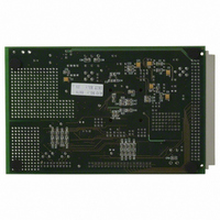
EVAL-AD7725CBZ Analog Devices Inc, EVAL-AD7725CBZ Datasheet - Page 25

EVAL-AD7725CBZ
Manufacturer Part Number
EVAL-AD7725CBZ
Description
BOARD EVALUATION FOR AD7725
Manufacturer
Analog Devices Inc
Datasheet
1.AD7725BSZ.pdf
(28 pages)
Specifications of EVAL-AD7725CBZ
Number Of Adc's
1
Number Of Bits
16
Sampling Rate (per Second)
900k
Data Interface
Serial, Parallel
Inputs Per Adc
1 Differential
Input Range
±VREF
Power (typ) @ Conditions
615mW @ 900kSPS
Voltage Supply Source
Analog and Digital
Operating Temperature
-40°C ~ 85°C
Utilized Ic / Part
AD7725
Lead Free Status / RoHS Status
Lead free / RoHS Compliant
DAISY-CHAINING DEVICES
Several AD7725s can be daisy-chained/cascaded together.
This feature of the AD7725 reduces system demands as it
allows several devices to be configured using one serial data
stream. It also allows conversion data from several devices to
be read back by a single DSP as one serial data stream. When
devices are daisy-chained, configuration/conversion data flows
from device to device using the SDO/FSO and SDI/FSI pins of
each device. A specific daisy-chaining configuration file needs
to be developed using the filter design package Filter Wizard.
The following sections describe the daisy-chaining options the
user can choose.
Daisy-Chaining during Configuration
Several AD7725s can be daisy-chained together so that they can
all be configured from a common external serial EPROM or a
DSP. Filter Wizard allows the user to specify the number of
devices in the chain and to design a specific filter for each device.
REV. A
ANALOG
INPUT
Figure 30. Connection Diagram for Loading the
Default Filter in BFR Mode
9.6MHz
CLKIN
DV
DD
Figure 31. Flow Chart of BFR Mode
DEVICE1
FILTER1
DEC
FROM INTERNAL ROM
POWER-ON RESET
POSTPROCESSOR
IMMEDIATE BOOT
DEFAULT FILTER
DEVICE STARTS
LOADED INTO
CONVERTING
FROM ROM
6
S/P
ERR
RESETCFG
CFGEND
INIT
DVAL
SOE
SMODE0
SMODE1
SYNC
INTERLACER
CFGEND = 1
INIT = 1
AD7725
SCO
SDO
FSO
SDI
FSI
SMODE0 = 0
SMODE1 = 0
ANALOG
INPUT
DIGITAL
INPUT
ADSP-21xx
SCLK0
RFS0
DR0
DT0
TFS0
DEVICE2
Figure 32. Daisy-Chaining Example
FILTER2
DEC
6
INTERLACER
–25–
It then generates a separate configuration file for each device.
The configuration files for all the devices can be combined
into one configuration file in order, starting with the file for
the first device, (for example, with a text editor) so that the
user only has to load one file into the EPROM or DSP. This
configuration file is loaded into the devices using the FSI/SDI
and the FSO/SDO of each device. Once the devices have been
configured in a daisy chain, each device can be run indepen-
dently, and conversion data is read back using the FSO and
SDO from each device separately.
Daisy-Chaining—Configuration and Conversion Data
Several AD7725s can be daisy-chained so that they are con-
figured from a common external serial EPROM or DSP (as
discussed earlier in Daisy-Chaining during Configuration),
and all conversion data from each individual device can be
read back by a single DSP on one serial data stream. To do
this, an interlacer is required following each filter on each
device. This design can be implemented using Filter Wizard.
The function of the interlacer is to sequentially combine the
conversion data outputs of each device into one serial data
stream. The interlacer combines the data using interpolation
and summing. Interpolation pads the data with zeros; then the
interlacer takes the output data from the previous device, delays
it by one clock cycle and sums it with the interpolated output
from the current device. This occurs on each device in the chain,
and the output data from the last device consists of the conver-
sion data from all devices in one continuous data stream. When
designing filters with interlacing, the decimation rate of the filter
on each device should be twice the number of devices in the
chain, or a multiple of this value, to ensure there is no interfer-
ence between the conversion data of different devices. Due to
the interpolation and decimation, the effective output data rate
of each device (out of the last device) is CLKIN/(16
of devices) and the actual output data rate of the final device is
CLKIN/16. Once the daisy-chaining and interlacing design is
complete, one configuration file is generated to be loaded into
the devices. Figure 32 shows an example of daisy-chaining three
devices, using interlacing.
Loading Configuration Data
When loading the configuration file from a common EPROM or
DSP, the configuration data is loaded into the first device in the
chain. Once this device is configured, the data will be loaded
into the second device in the chain via FSO/SDO of Device 1
and FSI/SDI of Device 2. When this device is configured,
the data is loaded into the next device in the chain until all
devices are configured. The CFGEND pin of the last device is
connected to the INIT pin of all the devices so that when the
last device is successfully configured, conversions are initiated.
ANALOG
INPUT
DIGITAL
INPUT
DEVICE3
FILTER3
DEC
6
INTERLACER
EFFECTIVE DATA OUTPUT RATE
FROM EACH DEVICE:
= CLKIN/(16
= 200kSPS
DATA OUTPUT FORMAT:
DEVICE3, DEVICE2,
DEVICE1; DEVICE3, ...
DATA OUTPUT
RATE = CLKIN/16
3)
AD7725
number


