EVAL-AD7944EBZ Analog Devices Inc, EVAL-AD7944EBZ Datasheet - Page 7
EVAL-AD7944EBZ
Manufacturer Part Number
EVAL-AD7944EBZ
Description
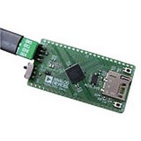
BOARD EVAL FOR AD7944
Manufacturer
Analog Devices Inc
Series
PulSAR®r
Datasheet
1.AD7944BCPZ.pdf
(28 pages)
Specifications of EVAL-AD7944EBZ
Number Of Adc's
1
Number Of Bits
14
Sampling Rate (per Second)
2.5M
Data Interface
SPI™, QSPI™, MICROWIRE™, and DSP
Inputs Per Adc
1 Differential
Input Range
0 ~ 5 V
Voltage Supply Source
Analog and Digital
Operating Temperature
-40°C ~ 85°C
Utilized Ic / Part
AD7944
Silicon Manufacturer
Analog Devices
Application Sub Type
ADC
Kit Application Type
Data Converter
Silicon Core Number
AD7944
Kit Contents
Board And Literature
Lead Free Status / RoHS Status
Lead free / RoHS Compliant


PIN CONFIGURATION AND FUNCTION DESCRIPTIONS
Table 6. Pin Function Descriptions
Pin No.
1, 2
3, 4
5
6
7
8
9
10
11
12
13
14
15
16
17, 18
Mnemonic
REF
REFGND
IN−
IN+
PDREF
VIO
SDO
DGND
DVDD
SCK
CNV
SDI
TURBO
AVDD
AGND
Type
AI
AI
AI
AI
DI
P
DO
P
P
DI
DI
DI
DI
P
P
1
Description
Reference Output/Input Voltage.
When PDREF is low, the internal reference and buffer are enabled, producing 4.096 V on this pin.
When PDREF is high, the internal reference and buffer are disabled, allowing an externally supplied
voltage reference up to 5.0 V.
Decoupling is required with or without the internal reference and buffer. This pin is referred to the
REFGND pins and should be decoupled closely to the REFGND pins with a 10 µF capacitor.
Reference Input Analog Ground.
Analog Input Ground Sense. Connect this pin to the analog ground plane or to a remote ground sense.
Analog Input. This pin is referred to IN −. The voltage range, that is, the difference between IN+ and IN−,
is 0 V to V
Internal Reference Power-Down Input. When this pin is low, the internal reference is enabled. When this
pin is high, the internal reference is powered down and an external reference must be used.
Input/Output Interface Digital Power. Nominally at the same supply voltage as the host interface
(1.8 V, 2.5 V, or 2.7 V).
Serial Data Output. The conversion result is output on this pin. It is synchronized to SCK.
Digital Power Ground.
Digital Power. Nominally at 2.5 V.
Serial Data Clock Input. When the part is selected, the conversion result is shifted out by this clock.
Convert Input. This input has multiple functions. On its rising edge, it initiates the conversions
and selects the interface mode of the part: chain mode or CS mode. In CS mode, the SDO pin is
enabled when CNV is low. In chain mode, the data should be read when CNV is high.
Serial Data Input. This input has multiple functions. It selects the interface mode of the ADC as follows.
Chain mode is selected if SDI is low during the CNV rising edge. In chain mode, SDI is used as a data
input to daisy-chain the conversion results of two or more ADCs onto a single SDO line. The digital data
level on SDI is output on SDO with a delay of 14 SCK cycles.
CS mode is selected if SDI is high during the CNV rising edge. In CS mode, either SDI or CNV can enable
the serial output signals when low. If SDI or CNV is low when the conversion is complete, the busy
indicator feature is enabled.
Conversion Mode Selection. When TURBO is high, the maximum throughput (2.5 MSPS) is achieved,
and the ADC does not power down between conversions. When TURBO is low, the maximum throughput
is lower (2.0 MSPS), and the ADC powers down between conversions.
Input Analog Power. Nominally at 2.5 V.
Analog Power Ground.
REF
.
NOTES
1. THE EXPOSED PAD IS NOT CONNECTED
REFGND
REFGND
INTERNALLY. FOR INCREASED
RELIABILITY OF THE SOLDER JOINTS, IT
IS RECOMMENDED THAT THE PAD BE
SOLDERED TO THE SYSTEM
GROUND PLANE.
REF
REF
IN–
Figure 4. Pin Configuration
1
2
3
4
5
Rev. A | Page 7 of 28
(Not to Scale)
AD7944
TOP VIEW
PIN 1
INDICATOR
15 TURBO
14 SDI
13 CNV
12 SCK
11 DVDD
AD7944
Related parts for EVAL-AD7944EBZ
Image
Part Number
Description
Manufacturer
Datasheet
Request
R


Part Number:
Description:
BOARD EVAL FOR SI270X-A
Manufacturer:
Silicon Laboratories Inc
Datasheet:

Part Number:
Description:
BUCK CONV REF DESIGN KIT IP1201
Manufacturer:
International Rectifier
Datasheet:
Part Number:
Description:
BOARD DEMO SYNC DUAL BUCK CNVTER
Manufacturer:
International Rectifier
Datasheet:
Part Number:
Description:
BOARD DEMO SYNC BUCK CONVETER
Manufacturer:
International Rectifier
Datasheet:

Part Number:
Description:
EVALBOARD/EB Omnidirectional microphone - Analog
Manufacturer:
Analog Devices
Datasheet:
Part Number:
Description:
EVALBOARD/EB Omnidirectional microphone - Analog
Manufacturer:
Analog Devices
Datasheet:


Part Number:
Description:
BOARD EVAL LED DRIVER LT3756
Manufacturer:
Linear Technology
Datasheet:

Part Number:
Description:
BOARD EVAL FOR AD7741/7742
Manufacturer:
Analog Devices Inc
Datasheet:

Part Number:
Description:
±1.7g Dual-Axis IMEMS Accelerometer Evaluation Board
Manufacturer:
Analog Devices Inc
Datasheet:

Part Number:
Description:
IC MULTIPLIER ANALOG 8-SOIC T/R
Manufacturer:
Analog Devices Inc
Datasheet:

Part Number:
Description:
IC ANALOG MULTIPLIER 8-DIP
Manufacturer:
Analog Devices Inc
Datasheet:
Part Number:
Description:
IC ANALOG MULTIPLIER 8-SOIC
Manufacturer:
Analog Devices Inc
Datasheet:
Part Number:
Description:
IC ANALOG MULTIPLIER 8-DIP
Manufacturer:
Analog Devices Inc
Datasheet: