EVAL-AD7944EBZ Analog Devices Inc, EVAL-AD7944EBZ Datasheet - Page 16
EVAL-AD7944EBZ
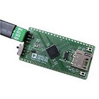
Manufacturer Part Number
EVAL-AD7944EBZ
Description
BOARD EVAL FOR AD7944
Manufacturer
Analog Devices Inc
Series
PulSAR®r
Datasheet
1.AD7944BCPZ.pdf
(28 pages)
Specifications of EVAL-AD7944EBZ
Number Of Adc's
1
Number Of Bits
14
Sampling Rate (per Second)
2.5M
Data Interface
SPI™, QSPI™, MICROWIRE™, and DSP
Inputs Per Adc
1 Differential
Input Range
0 ~ 5 V
Voltage Supply Source
Analog and Digital
Operating Temperature
-40°C ~ 85°C
Utilized Ic / Part
AD7944
Silicon Manufacturer
Analog Devices
Application Sub Type
ADC
Kit Application Type
Data Converter
Silicon Core Number
AD7944
Kit Contents
Board And Literature
Lead Free Status / RoHS Status
Lead free / RoHS Compliant


AD7944
VOLTAGE REFERENCE INPUT
The AD7944 allows the choice of a very low temperature drift
internal voltage reference, an external reference, or an external
buffered reference.
The internal reference of the AD7944 provides excellent
performance and can be used in almost all applications.
Internal Reference, REF = 4.096 V (PDREF Low)
To use the internal reference, the PDREF input must be low.
This enables the on-chip band gap reference and buffer, result-
ing in a 4.096 V reference on the REF pin (1.2 V on REFIN).
The internal reference is temperature compensated to
4.096 V ± 15 mV. The reference is trimmed to provide
a typical drift of 10 ppm/°C.
The output resistance of REFIN is 6 kΩ when the internal
reference is enabled. It is necessary to decouple this pin with a
ceramic capacitor of at least 100 nF. The output resistance of
REFIN and the decoupling capacitor form an RC filter, which
helps to reduce noise.
Because the output impedance of REFIN is typically 6 kΩ,
relative humidity (among other industrial contaminants) can
directly affect the drift characteristics of the reference. A guard
ring is typically used to reduce the effects of drift under such
circumstances. However, the fine pitch of the AD7944 makes
this difficult to implement. One solution, in these industrial
and other types of applications, is to use a conformal coating,
such as Dow Corning® 1-2577 or HumiSeal® 1B73.
External 1.2 V Reference and Internal Buffer (PDREF High)
To use an external reference along with the internal buffer, PDREF
must be high. This powers down the internal reference and allows
the 1.2 V reference to be applied to REFIN, producing 4.096 V
(typically) on the REF pin.
External Reference (PDREF High, REFIN Low)
To apply an external reference voltage directly to the REF pin, tie
PDREF high and tie REFIN low. BVDD should also be driven to
the same potential as REF. For example, if REF = 2.5 V, BVDD
should be tied to 2.5 V.
The advantages of directly using an external voltage reference
are as follows:
•
•
SNR and dynamic range improvement (about 1.7 dB)
resulting from the use of a larger reference voltage (5 V)
instead of a typical 4.096 V reference when the internal
reference is used. This is calculated by
Power savings when the internal reference is powered
down (PDREF high).
SNR
=
20
log
. 4
5
096
0 .
Rev. A | Page 16 of 28
Reference Decoupling
The AD7944 voltage reference input, REF, has a dynamic input
impedance that requires careful decoupling between the REF
and REFGND pins. The Layout section describes how this can
be done.
When using an external reference, a very low impedance source
(for example, a reference buffer using the
and a 10 µF (X5R, 0805 size) ceramic chip capacitor are appro-
priate for optimum performance.
If an unbuffered reference voltage is used, the decoupling value
depends on the reference used. For example, a 22 µF (X5R,
1206 size) ceramic chip capacitor is appropriate for optimum
performance using a low temperature drift
If desired, a reference decoupling capacitor with a value as small
as 2.2 µF can be used with minimal impact on performance,
especially DNL.
In any case, there is no need for an additional, lower value
ceramic decoupling capacitor (for example, 100 nF) between
the REF and REFGND pins.
POWER SUPPLY
The AD7944 has four power supply pins: an analog supply
(AVDD), a buffer supply (BVDD), a digital supply (DVDD), and
a digital input/output interface supply (VIO). VIO allows a direct
interface to any logic from 1.8 V to 2.7 V. To reduce the number
of supplies needed, the VIO, DVDD, and AVDD pins can be
tied together. The power supplies do not need to be started in a
particular sequence. In addition, the AD7944 is very insensitive
to power supply variations over a wide frequency range.
In normal mode, the AD7944 powers down automatically at
the end of each conversion phase and, therefore, the power
scales linearly with the sampling rate. This makes the part ideal
for low sampling rates (even of a few SPS) and battery-powered
applications.
Figure 25. Operating Current vs. Sampling Rate in Normal Mode
0.01
0.1
10
1
0.1
SAMPLING RATE (MSPS)
AD8031
ADR43x
1
or the AD8605)
I
I
I
I
I
reference.
BVDD
AVDD
DVDD
VIO
VREF
Related parts for EVAL-AD7944EBZ
Image
Part Number
Description
Manufacturer
Datasheet
Request
R


Part Number:
Description:
BOARD EVAL FOR SI270X-A
Manufacturer:
Silicon Laboratories Inc
Datasheet:

Part Number:
Description:
BUCK CONV REF DESIGN KIT IP1201
Manufacturer:
International Rectifier
Datasheet:
Part Number:
Description:
BOARD DEMO SYNC DUAL BUCK CNVTER
Manufacturer:
International Rectifier
Datasheet:
Part Number:
Description:
BOARD DEMO SYNC BUCK CONVETER
Manufacturer:
International Rectifier
Datasheet:

Part Number:
Description:
EVALBOARD/EB Omnidirectional microphone - Analog
Manufacturer:
Analog Devices
Datasheet:
Part Number:
Description:
EVALBOARD/EB Omnidirectional microphone - Analog
Manufacturer:
Analog Devices
Datasheet:


Part Number:
Description:
BOARD EVAL LED DRIVER LT3756
Manufacturer:
Linear Technology
Datasheet:

Part Number:
Description:
BOARD EVAL FOR AD7741/7742
Manufacturer:
Analog Devices Inc
Datasheet:

Part Number:
Description:
±1.7g Dual-Axis IMEMS Accelerometer Evaluation Board
Manufacturer:
Analog Devices Inc
Datasheet:

Part Number:
Description:
IC MULTIPLIER ANALOG 8-SOIC T/R
Manufacturer:
Analog Devices Inc
Datasheet:

Part Number:
Description:
IC ANALOG MULTIPLIER 8-DIP
Manufacturer:
Analog Devices Inc
Datasheet:
Part Number:
Description:
IC ANALOG MULTIPLIER 8-SOIC
Manufacturer:
Analog Devices Inc
Datasheet:
Part Number:
Description:
IC ANALOG MULTIPLIER 8-DIP
Manufacturer:
Analog Devices Inc
Datasheet: