EVAL-AD7944EBZ Analog Devices Inc, EVAL-AD7944EBZ Datasheet - Page 19
EVAL-AD7944EBZ
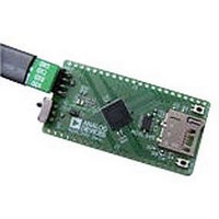
Manufacturer Part Number
EVAL-AD7944EBZ
Description
BOARD EVAL FOR AD7944
Manufacturer
Analog Devices Inc
Series
PulSAR®r
Datasheet
1.AD7944BCPZ.pdf
(28 pages)
Specifications of EVAL-AD7944EBZ
Number Of Adc's
1
Number Of Bits
14
Sampling Rate (per Second)
2.5M
Data Interface
SPI™, QSPI™, MICROWIRE™, and DSP
Inputs Per Adc
1 Differential
Input Range
0 ~ 5 V
Voltage Supply Source
Analog and Digital
Operating Temperature
-40°C ~ 85°C
Utilized Ic / Part
AD7944
Silicon Manufacturer
Analog Devices
Application Sub Type
ADC
Kit Application Type
Data Converter
Silicon Core Number
AD7944
Kit Contents
Board And Literature
Lead Free Status / RoHS Status
Lead free / RoHS Compliant


CS MODE, 3-WIRE WITHOUT BUSY INDICATOR
This mode is usually used when a single AD7944 is connected
to an SPI-compatible digital host. The connection diagram is
shown in Figure 26, and the corresponding timing is given in
Figure 27.
With SDI tied to VIO, a rising edge on CNV initiates a con-
version, selects CS mode, and forces SDO to high impedance.
When a conversion is initiated, it continues until completion,
irrespective of the state of CNV. This can be useful, for example,
to bring CNV low to select other SPI devices, such as analog
multiplexers; however, CNV must be returned high before the
ACQUISITION
SDI = 1
CNV
(n – 1)
SCK
SDO
t
DIS
END DATA (n – 2)
CONVERSION (n – 1)
t
EN
t
DATA
12
2
>
t
CONV
13
t
CONV
1
14
Figure 27. CS Mode, 3-Wire Without Busy Indicator Serial Interface Timing (SDI High)
Figure 26. CS Mode, 3-Wire Without Busy Indicator Connection Diagram (SDI High)
0
t
(I/O QUIET
DIS
TIME)
VIO
t
CYC
SDI
t
EN
AD7944
CNV
SCK
13
1
Rev. A | Page 19 of 28
ACQUISITION (n)
12
2
t
SDO
ACQ
BEGIN DATA (n – 1)
11
t
t
HSDO
DSDO
minimum conversion time elapses and then held high for the
maximum possible conversion time to avoid the generation of
the busy signal indicator.
When the conversion is complete, the AD7944 enters the
acquisition phase and, if the part is in normal mode (TURBO
low), powers down. When CNV goes low, the MSB is output
onto SDO. The remaining data bits are clocked by subsequent
SCK falling edges. The data is valid on both SCK edges. Although
the rising edge can be used to capture the data, a digital host
using the SCK falling edge allows a faster reading rate, provided
that it has an acceptable hold time. After the 14
edge or when CNV goes high (whichever occurs first), SDO
returns to high impedance.
CONVERT
DATA IN
CLK
DIGITAL HOST
(I/O QUIET
TIME)
t
QUIET
t
DIS
CONVERSION (n)
END DATA (n – 1)
t
CNVH
12
t
2
DATA
t
CONV
13
1
t
SCK
14
0
t
(I/O QUIET
DIS
TIME)
th
SCK falling
ACQUISITION
AD7944
(n + 1)
Related parts for EVAL-AD7944EBZ
Image
Part Number
Description
Manufacturer
Datasheet
Request
R


Part Number:
Description:
BOARD EVAL FOR SI270X-A
Manufacturer:
Silicon Laboratories Inc
Datasheet:

Part Number:
Description:
BUCK CONV REF DESIGN KIT IP1201
Manufacturer:
International Rectifier
Datasheet:
Part Number:
Description:
BOARD DEMO SYNC DUAL BUCK CNVTER
Manufacturer:
International Rectifier
Datasheet:
Part Number:
Description:
BOARD DEMO SYNC BUCK CONVETER
Manufacturer:
International Rectifier
Datasheet:

Part Number:
Description:
EVALBOARD/EB Omnidirectional microphone - Analog
Manufacturer:
Analog Devices
Datasheet:
Part Number:
Description:
EVALBOARD/EB Omnidirectional microphone - Analog
Manufacturer:
Analog Devices
Datasheet:


Part Number:
Description:
BOARD EVAL LED DRIVER LT3756
Manufacturer:
Linear Technology
Datasheet:

Part Number:
Description:
BOARD EVAL FOR AD7741/7742
Manufacturer:
Analog Devices Inc
Datasheet:

Part Number:
Description:
±1.7g Dual-Axis IMEMS Accelerometer Evaluation Board
Manufacturer:
Analog Devices Inc
Datasheet:

Part Number:
Description:
IC MULTIPLIER ANALOG 8-SOIC T/R
Manufacturer:
Analog Devices Inc
Datasheet:

Part Number:
Description:
IC ANALOG MULTIPLIER 8-DIP
Manufacturer:
Analog Devices Inc
Datasheet:
Part Number:
Description:
IC ANALOG MULTIPLIER 8-SOIC
Manufacturer:
Analog Devices Inc
Datasheet:
Part Number:
Description:
IC ANALOG MULTIPLIER 8-DIP
Manufacturer:
Analog Devices Inc
Datasheet: