ADC1415S125/DB,598 NXP Semiconductors, ADC1415S125/DB,598 Datasheet - Page 9
ADC1415S125/DB,598
Manufacturer Part Number
ADC1415S125/DB,598
Description
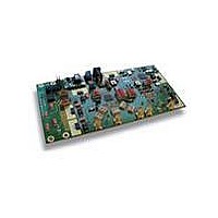
BOARD DEMO FOR ADC1415S125
Manufacturer
NXP Semiconductors
Type
A/Dr
Datasheets
1.ADC1415S125HNC15.pdf
(42 pages)
2.HSDC-ACC01DB.pdf
(32 pages)
3.ADC1415S125DB598.pdf
(2 pages)
Specifications of ADC1415S125/DB,598
Number Of Adc's
1
Number Of Bits
14
Sampling Rate (per Second)
125M
Data Interface
Serial, SPI™
Inputs Per Adc
1 Differential
Input Range
1 ~ 2 Vpp
Power (typ) @ Conditions
840mW @ 125Msps
Voltage Supply Source
Single Supply
Operating Temperature
-40°C ~ 85°C
Utilized Ic / Part
ADC1415S125
Product
Data Conversion Development Tools
Conversion Rate
125 MSPS
Resolution
14 bit
Interface Type
SMA
For Use With/related Products
ADC1415S125
Lead Free Status / RoHS Status
Lead free / RoHS Compliant
Lead Free Status / RoHS Status
Lead free / RoHS Compliant, Lead free / RoHS Compliant
Other names
568-5094


NXP Semiconductors
Table 6.
[1]
ADC1415S_SER
Product data sheet
Symbol
Accuracy
INL
DNL
E
E
Supply
PSRR
offset
G
Typical values measured at V
are across the full temperature range T
internal reference mode; applied to CMOS and LVDS interface; unless otherwise specified.
Static characteristics
Parameter
integral non-linearity
differential non-linearity
offset error
gain error
power supply rejection ratio
DDA(3V)
[1]
…continued
= 3 V, V
amb
All information provided in this document is subject to legal disclaimers.
= −40 °C to +85 °C at V
Single 14-bit ADC; input buffer; CMOS or LVDS DDR digital outputs
DDO
= 1.8 V, V
Rev. 4 — 17 December 2010
Conditions
guaranteed no
missing codes
200 mV (p-p) on
V
DDA(3V)
DDA(5V)
= 5 V; T
DDA(3V)
= 3 V, V
amb
= 25 °C and C
Min
−5
−0.95
-
-
-
DDO
= 1.8 V, V
ADC1415S series
L
= 5 pF; minimum and maximum values
Typ
-
±0.5
±2
±0.5
−54
DDA(5V)
= 5 V, V
Max
+5
+0.95
-
-
-
INP
© NXP B.V. 2010. All rights reserved.
− V
INM
= −1 dBFS;
Unit
LSB
LSB
mV
%FS
dBc
9 of 42
Related parts for ADC1415S125/DB,598
Image
Part Number
Description
Manufacturer
Datasheet
Request
R

Part Number:
Description:
Single 14-bit ADC
Manufacturer:
NXP Semiconductors
Datasheet:
Part Number:
Description:
NXP Semiconductors designed the LPC2420/2460 microcontroller around a 16-bit/32-bitARM7TDMI-S CPU core with real-time debug interfaces that include both JTAG andembedded trace
Manufacturer:
NXP Semiconductors
Datasheet:

Part Number:
Description:
NXP Semiconductors designed the LPC2458 microcontroller around a 16-bit/32-bitARM7TDMI-S CPU core with real-time debug interfaces that include both JTAG andembedded trace
Manufacturer:
NXP Semiconductors
Datasheet:
Part Number:
Description:
NXP Semiconductors designed the LPC2468 microcontroller around a 16-bit/32-bitARM7TDMI-S CPU core with real-time debug interfaces that include both JTAG andembedded trace
Manufacturer:
NXP Semiconductors
Datasheet:
Part Number:
Description:
NXP Semiconductors designed the LPC2470 microcontroller, powered by theARM7TDMI-S core, to be a highly integrated microcontroller for a wide range ofapplications that require advanced communications and high quality graphic displays
Manufacturer:
NXP Semiconductors
Datasheet:
Part Number:
Description:
NXP Semiconductors designed the LPC2478 microcontroller, powered by theARM7TDMI-S core, to be a highly integrated microcontroller for a wide range ofapplications that require advanced communications and high quality graphic displays
Manufacturer:
NXP Semiconductors
Datasheet:
Part Number:
Description:
The Philips Semiconductors XA (eXtended Architecture) family of 16-bit single-chip microcontrollers is powerful enough to easily handle the requirements of high performance embedded applications, yet inexpensive enough to compete in the market for hi
Manufacturer:
NXP Semiconductors
Datasheet:
Part Number:
Description:
The XA-S3 device is a member of Philips Semiconductors? XA(eXtended Architecture) family of high performance 16-bitsingle-chip microcontrollers
Manufacturer:
NXP Semiconductors
Datasheet:

Part Number:
Description:
The NXP BlueStreak LH75401/LH75411 family consists of two low-cost 16/32-bit System-on-Chip (SoC) devices
Manufacturer:
NXP Semiconductors
Datasheet:
Part Number:
Description:
The NXP LPC3130/3131 combine an 180 MHz ARM926EJ-S CPU core, high-speed USB2
Manufacturer:
NXP Semiconductors
Datasheet:
Part Number:
Description:
The NXP LPC3141 combine a 270 MHz ARM926EJ-S CPU core, High-speed USB 2
Manufacturer:
NXP Semiconductors
Part Number:
Description:
The NXP LPC3143 combine a 270 MHz ARM926EJ-S CPU core, High-speed USB 2
Manufacturer:
NXP Semiconductors

Part Number:
Description:
The NXP LPC3152 combines an 180 MHz ARM926EJ-S CPU core, High-speed USB 2
Manufacturer:
NXP Semiconductors
Part Number:
Description:
The NXP LPC3154 combines an 180 MHz ARM926EJ-S CPU core, High-speed USB 2
Manufacturer:
NXP Semiconductors