ADC1415S125/DB,598 NXP Semiconductors, ADC1415S125/DB,598 Datasheet - Page 28
ADC1415S125/DB,598
Manufacturer Part Number
ADC1415S125/DB,598
Description
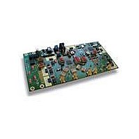
BOARD DEMO FOR ADC1415S125
Manufacturer
NXP Semiconductors
Type
A/Dr
Datasheets
1.ADC1415S125HNC15.pdf
(42 pages)
2.HSDC-ACC01DB.pdf
(32 pages)
3.ADC1415S125DB598.pdf
(2 pages)
Specifications of ADC1415S125/DB,598
Number Of Adc's
1
Number Of Bits
14
Sampling Rate (per Second)
125M
Data Interface
Serial, SPI™
Inputs Per Adc
1 Differential
Input Range
1 ~ 2 Vpp
Power (typ) @ Conditions
840mW @ 125Msps
Voltage Supply Source
Single Supply
Operating Temperature
-40°C ~ 85°C
Utilized Ic / Part
ADC1415S125
Product
Data Conversion Development Tools
Conversion Rate
125 MSPS
Resolution
14 bit
Interface Type
SMA
For Use With/related Products
ADC1415S125
Lead Free Status / RoHS Status
Lead free / RoHS Compliant
Lead Free Status / RoHS Status
Lead free / RoHS Compliant, Lead free / RoHS Compliant
Other names
568-5094


NXP Semiconductors
ADC1415S_SER
Product data sheet
11.5.7 Output codes versus input voltage
11.6.1 Register description
11.6 Serial Peripheral Interface (SPI)
Table 15.
The ADC1415S serial interface is a synchronous serial communications port that allows
easy interfacing with many commonly-used microprocessors. It provides access to the
registers that control the operation of the chip.
This interface is configured as a 3-wire type (SDIO as bidirectional pin)
Pin SCLK is the serial clock input and CS is the chip select pin.
Each read/write operation is initiated by a LOW level on CS. A minimum of three bytes is
transmitted (two instruction bytes and at least one data byte). The number of data bytes is
determined by the value of bits W1 and W2 (see
Table 16.
[1]
[2]
V
< −1
−1
−0.9998779
−0.9997559
−0.9996338
−0.9995117
....
−0.0002441
−0.0001221
0
+0.0001221
+0.0002441
....
+0.9995117
+0.9996338
+0.9997559
+0.9998779
+1
> +1
Bit
Description
INP
Bit R/W indicates whether it is a read (logic 1) or a write (logic 0) operation.
Bits W1 and W0 indicate the number of bytes to be transferred after the instruction byte (see
− V
INM
Output codes
Instruction bytes for the SPI
Offset binary
00 0000 0000 0000
00 0000 0000 0000
00 0000 0000 0001
00 0000 0000 0010
00 0000 0000 0011
00 0000 0000 0100
....
01 1111 1111 1110
01 1111 1111 1111
10 0000 0000 0000
10 0000 0000 0001
10 0000 0000 0010
....
11 1111 1111 1011
11 1111 1111 1100
11 1111 1111 1101
11 1111 1111 1110
11 1111 1111 1111
11 1111 1111 1111
All information provided in this document is subject to legal disclaimers.
Single 14-bit ADC; input buffer; CMOS or LVDS DDR digital outputs
MSB
7
A7
R/W
Rev. 4 — 17 December 2010
[1]
6
W1
A6
[2]
5
W0
A5
[2]
4
A12
A4
Table
Two’s complement
10 0000 0000 0000
10 0000 0000 0000
10 0000 0000 0001
10 0000 0000 0010
10 0000 0000 0011
10 0000 0000 0100
....
11 1111 1111 1110
11 1111 1111 1111
00 0000 0000 0000
00 0000 0000 0001
00 0000 0000 0010
....
01 1111 1111 1011
01 1111 1111 1100
01 1111 1111 1101
01 1111 1111 1110
01 1111 1111 1111
01 1111 1111 1111
ADC1415S series
3
A11
A3
17).
2
A10
A2
© NXP B.V. 2010. All rights reserved.
1
A9
A1
OTR pin
1
0
0
0
0
0
0
0
0
0
0
0
0
0
0
0
0
0
1
Table
LSB
0
A8
A0
28 of 42
17).
Related parts for ADC1415S125/DB,598
Image
Part Number
Description
Manufacturer
Datasheet
Request
R

Part Number:
Description:
Single 14-bit ADC
Manufacturer:
NXP Semiconductors
Datasheet:
Part Number:
Description:
NXP Semiconductors designed the LPC2420/2460 microcontroller around a 16-bit/32-bitARM7TDMI-S CPU core with real-time debug interfaces that include both JTAG andembedded trace
Manufacturer:
NXP Semiconductors
Datasheet:

Part Number:
Description:
NXP Semiconductors designed the LPC2458 microcontroller around a 16-bit/32-bitARM7TDMI-S CPU core with real-time debug interfaces that include both JTAG andembedded trace
Manufacturer:
NXP Semiconductors
Datasheet:
Part Number:
Description:
NXP Semiconductors designed the LPC2468 microcontroller around a 16-bit/32-bitARM7TDMI-S CPU core with real-time debug interfaces that include both JTAG andembedded trace
Manufacturer:
NXP Semiconductors
Datasheet:
Part Number:
Description:
NXP Semiconductors designed the LPC2470 microcontroller, powered by theARM7TDMI-S core, to be a highly integrated microcontroller for a wide range ofapplications that require advanced communications and high quality graphic displays
Manufacturer:
NXP Semiconductors
Datasheet:
Part Number:
Description:
NXP Semiconductors designed the LPC2478 microcontroller, powered by theARM7TDMI-S core, to be a highly integrated microcontroller for a wide range ofapplications that require advanced communications and high quality graphic displays
Manufacturer:
NXP Semiconductors
Datasheet:
Part Number:
Description:
The Philips Semiconductors XA (eXtended Architecture) family of 16-bit single-chip microcontrollers is powerful enough to easily handle the requirements of high performance embedded applications, yet inexpensive enough to compete in the market for hi
Manufacturer:
NXP Semiconductors
Datasheet:
Part Number:
Description:
The XA-S3 device is a member of Philips Semiconductors? XA(eXtended Architecture) family of high performance 16-bitsingle-chip microcontrollers
Manufacturer:
NXP Semiconductors
Datasheet:

Part Number:
Description:
The NXP BlueStreak LH75401/LH75411 family consists of two low-cost 16/32-bit System-on-Chip (SoC) devices
Manufacturer:
NXP Semiconductors
Datasheet:
Part Number:
Description:
The NXP LPC3130/3131 combine an 180 MHz ARM926EJ-S CPU core, high-speed USB2
Manufacturer:
NXP Semiconductors
Datasheet:
Part Number:
Description:
The NXP LPC3141 combine a 270 MHz ARM926EJ-S CPU core, High-speed USB 2
Manufacturer:
NXP Semiconductors
Part Number:
Description:
The NXP LPC3143 combine a 270 MHz ARM926EJ-S CPU core, High-speed USB 2
Manufacturer:
NXP Semiconductors

Part Number:
Description:
The NXP LPC3152 combines an 180 MHz ARM926EJ-S CPU core, High-speed USB 2
Manufacturer:
NXP Semiconductors
Part Number:
Description:
The NXP LPC3154 combines an 180 MHz ARM926EJ-S CPU core, High-speed USB 2
Manufacturer:
NXP Semiconductors