ADCLK950/PCBZ Analog Devices Inc, ADCLK950/PCBZ Datasheet - Page 5
ADCLK950/PCBZ
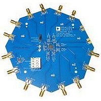
Manufacturer Part Number
ADCLK950/PCBZ
Description
BOARD EVALUATION FOR ADCLK950
Manufacturer
Analog Devices Inc
Series
SIGer
Specifications of ADCLK950/PCBZ
Main Purpose
Timing, Clock Buffer / Driver / Receiver / Translator
Utilized Ic / Part
ADCLK950
Primary Attributes
2 Selectable Inputs, 10 Outputs
Secondary Attributes
LVPECL Output Logic
Silicon Manufacturer
Analog Devices
Application Sub Type
Clock Fanout Buffer
Kit Application Type
Clock & Timing
Silicon Core Number
ADCLK950
Lead Free Status / RoHS Status
Lead free / RoHS Compliant
Embedded
-
Lead Free Status / RoHS Status
Lead free / RoHS Compliant


ABSOLUTE MAXIMUM RATINGS
Table 5.
Parameter
Supply Voltage
Input Voltage
Maximum Voltage on Output Pins
Maximum Output Current
Voltage Reference (V
Operating Temperature Range
Storage Temperature Range
Stresses above those listed under Absolute Maximum Ratings
may cause permanent damage to the device. This is a stress
rating only; functional operation of the device at these or any
other conditions above those indicated in the operational
section of this specification is not implied. Exposure to absolute
maximum rating conditions for extended periods may affect
device reliability.
THERMAL PERFORMANCE
Table 6.
Parameter
Junction-to-Ambient Thermal Resistance
Junction-to-Board Thermal Resistance
Junction-to-Case Thermal Resistance
Junction-to-Top-of-Package Characterization Parameter
1
Results are from simulations. The PCB is a JEDEC multilayer type. Thermal performance for actual applications requires careful inspection of the conditions in the
application to determine if they are similar to those assumed in these calculations.
V
CLK0, CLK1, CLK0, CLK1, IN_SEL
Input Termination, V
Ambient
Junction
Still Air
Moving Air
Moving Air
Moving Air
Still Air
CLK0, CLK1, CLK0, CLK1 to V
CLK0, CLK1 to CLK0, CLK1
CC
and CLK1
0 m/sec Air Flow
1 m/sec Air Flow
2.5 m/sec Air Flow
1 m/sec Air Flow
Die-to-Heatsink
0 m/sec Air Flow
LVPECL Termination)
− V
EE
REF
T
x to CLK0, CLK1, CLK0,
x)
T
x Pin (CML,
Rating
6 V
V
V
±40 mA
±1.8 V
±2 V
V
35 mA
V
−40°C to +85°C
150°C
−65°C to +150°C
EE
CC
CC
CC
− 0.5 V to
+ 0.5 V
+ 0.5 V
to V
EE
Rev. A | Page 5 of 12
Symbol
θ
θ
θ
θ
Ψ
JA
JMA
JB
JC
JT
DETERMINING JUNCTION TEMPERATURE
To determine the junction temperature on the application
printed circuit board (PCB), use the following equation:
where:
the top center of the package.
Ψ is from Table 6.
Values of θ
design considerations. θ
mation of T
where
Values of θ
and PCB design considerations.
ESD CAUTION
is the junction temperature (°C).
is the power dissipation.
is the case temperature (°C) measured by the customer at
Description
Per JEDEC JESD51-2
Per JEDEC JESD51-6
Per JEDEC JESD51-8
Per MIL-STD 883, Method 1012.1
Per JEDEC JESD51-2
=
=
is the ambient temperature (°C).
JA
JB
J
+ (
by the equation
are provided in Table 6 for package comparison
are provided for package comparison and PCB
+ (Ψ ×
θ
×
)
JA
)
can be used for a first-order approxi-
Value
46.1
40.3
36.2
28.7
8.3
0.6
ADCLK950
1
Unit
°C/W
°C/W
°C/W
°C/W
°C/W
°C/W
Related parts for ADCLK950/PCBZ
Image
Part Number
Description
Manufacturer
Datasheet
Request
R

Part Number:
Description:
±1.7g Dual-Axis IMEMS Accelerometer Evaluation Board
Manufacturer:
Analog Devices Inc
Datasheet:

Part Number:
Description:
Inertial Sensor Evaluation System
Manufacturer:
Analog Devices Inc
Datasheet:
Part Number:
Description:
Manufacturer:
Analog Devices Inc
Datasheet:
Part Number:
Description:
Manufacturer:
Analog Devices Inc
Datasheet:
Part Number:
Description:
Manufacturer:
Analog Devices Inc
Datasheet:
Part Number:
Description:
Manufacturer:
Analog Devices Inc
Datasheet:
Part Number:
Description:
Manufacturer:
Analog Devices Inc
Datasheet:
Part Number:
Description:
Manufacturer:
Analog Devices Inc
Datasheet:
Part Number:
Description:
Manufacturer:
Analog Devices Inc
Datasheet:
Part Number:
Description:
Manufacturer:
Analog Devices Inc
Datasheet:
Part Number:
Description:
Manufacturer:
Analog Devices Inc
Datasheet:
Part Number:
Description:
Manufacturer:
Analog Devices Inc
Datasheet:
Part Number:
Description:
Manufacturer:
Analog Devices Inc
Datasheet: