ADCLK950/PCBZ Analog Devices Inc, ADCLK950/PCBZ Datasheet - Page 12
ADCLK950/PCBZ
Manufacturer Part Number
ADCLK950/PCBZ
Description
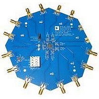
BOARD EVALUATION FOR ADCLK950
Manufacturer
Analog Devices Inc
Series
SIGer
Specifications of ADCLK950/PCBZ
Main Purpose
Timing, Clock Buffer / Driver / Receiver / Translator
Utilized Ic / Part
ADCLK950
Primary Attributes
2 Selectable Inputs, 10 Outputs
Secondary Attributes
LVPECL Output Logic
Silicon Manufacturer
Analog Devices
Application Sub Type
Clock Fanout Buffer
Kit Application Type
Clock & Timing
Silicon Core Number
ADCLK950
Lead Free Status / RoHS Status
Lead free / RoHS Compliant
Embedded
-
Lead Free Status / RoHS Status
Lead free / RoHS Compliant


ADCLK950
OUTLINE DIMENSIONS
ORDERING GUIDE
Model
ADCLK950BCPZ
ADCLK950BCPZ-REEL7
ADCLK950/PCBZ
1
©2009–2010 Analog Devices, Inc. All rights reserved. Trademarks and
registered trademarks are the property of their respective owners.
Z = RoHS Compliant Part.
1
SEATING
PLANE
1.00
0.85
0.80
INDICATOR
PIN 1
12° MAX
Temperature Range
−40°C to +85°C
−40°C to +85°C
D08279-0-6/10(A)
TOP VIEW
BSC SQ
Figure 24. 40-Lead Lead Frame Chip Scale Package [LFCSP_VQ]
6.00
0.30
0.23
0.18
0.80 MAX
0.65 TYP
COMPLIANT TO JEDEC STANDARDS MO-220-VJJD-2
6 mm × 6 mm Body, Very Thin Quad
Dimensions shown in millimeters
BSC SQ
0.20 REF
5.75
Rev. A | Page 12 of 12
0.05 MAX
0.02 NOM
COPLANARITY
(CP-40-8)
0.60 MAX
0.08
BSC
0.50
0.50
0.40
0.30
Package Description
40-Lead LFCSP_VQ
40-Lead LFCSP_VQ
Evaluation Board
28
20
29
19
BOTTOM VIEW
0.60 MAX
EXPOSED
4.50
PAD
REF
FOR PROPER CONNECTION OF
THE EXPOSED PAD, REFER TO
THE PIN CONFIGURATION AND
FUNCTION DESCRIPTIONS
SECTION OF THIS DATA SHEET.
11
40
10
1
0.25 MIN
PIN 1
INDICATOR
3.05
2.90 SQ
2.75
Package Option
CP-40-8
CP-40-8
Related parts for ADCLK950/PCBZ
Image
Part Number
Description
Manufacturer
Datasheet
Request
R

Part Number:
Description:
±1.7g Dual-Axis IMEMS Accelerometer Evaluation Board
Manufacturer:
Analog Devices Inc
Datasheet:

Part Number:
Description:
Inertial Sensor Evaluation System
Manufacturer:
Analog Devices Inc
Datasheet:
Part Number:
Description:
Manufacturer:
Analog Devices Inc
Datasheet:
Part Number:
Description:
Manufacturer:
Analog Devices Inc
Datasheet:
Part Number:
Description:
Manufacturer:
Analog Devices Inc
Datasheet:
Part Number:
Description:
Manufacturer:
Analog Devices Inc
Datasheet:
Part Number:
Description:
Manufacturer:
Analog Devices Inc
Datasheet:
Part Number:
Description:
Manufacturer:
Analog Devices Inc
Datasheet:
Part Number:
Description:
Manufacturer:
Analog Devices Inc
Datasheet:
Part Number:
Description:
Manufacturer:
Analog Devices Inc
Datasheet:
Part Number:
Description:
Manufacturer:
Analog Devices Inc
Datasheet:
Part Number:
Description:
Manufacturer:
Analog Devices Inc
Datasheet:
Part Number:
Description:
Manufacturer:
Analog Devices Inc
Datasheet: