ADCLK950/PCBZ Analog Devices Inc, ADCLK950/PCBZ Datasheet - Page 10
ADCLK950/PCBZ
Manufacturer Part Number
ADCLK950/PCBZ
Description
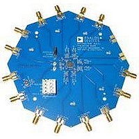
BOARD EVALUATION FOR ADCLK950
Manufacturer
Analog Devices Inc
Series
SIGer
Specifications of ADCLK950/PCBZ
Main Purpose
Timing, Clock Buffer / Driver / Receiver / Translator
Utilized Ic / Part
ADCLK950
Primary Attributes
2 Selectable Inputs, 10 Outputs
Secondary Attributes
LVPECL Output Logic
Silicon Manufacturer
Analog Devices
Application Sub Type
Clock Fanout Buffer
Kit Application Type
Clock & Timing
Silicon Core Number
ADCLK950
Lead Free Status / RoHS Status
Lead free / RoHS Compliant
Embedded
-
Lead Free Status / RoHS Status
Lead free / RoHS Compliant


ADCLK950
CLOCK INPUT SELECT (IN_SEL) SETTINGS
A Logic 0 on the IN_SEL pin selects the Input CLK0 and
Input CLK0 . A Logic 1 on the IN_SEL pin selects Input CLK1
and Input CLK1 .
PCB LAYOUT CONSIDERATIONS
The ADCLK950 buffer is designed for very high speed applica-
tions. Consequently, high speed design techniques must be used
to achieve the specified performance. It is critically important
to use low impedance supply planes for both the negative supply
(V
board. Providing the lowest inductance return path for switching
currents ensures the best possible performance in the target
application.
The following references to the GND plane assume that the V
power plane is grounded for LVPECL operation. Note that for
ECL operation, the V
It is also important to adequately bypass the input and output
supplies. Place a 1 μF electrolytic bypass capacitor within several
inches of each V
addition, place multiple high quality 0.001 μF bypass capacitors
as close as possible to each of the V
the capacitors to the GND plane with redundant vias. Carefully
select high frequency bypass capacitors for minimum induc-
tance and ESR. To improve the effectiveness of the bypass at
high frequencies, minimize parasitic layout inductance. Also,
avoid discontinuities along input and output transmission lines
that can affect jitter performance.
In a 50 Ω environment, input and output matching have a
significant impact on performance. The buffer provides internal
50 Ω termination resistors for both CLKx and CLKx inputs.
Normally, the return side is connected to the reference pin that is
provided. Carefully bypass the termination potential using
ceramic capacitors to prevent undesired aberrations on the
input signal due to parasitic inductance in the termination
EE
) and the positive supply (V
CC
power supply pin to the GND plane. In
CC
power plane becomes the ground plane.
CC
) planes as part of a multilayer
CC
supply pins, and connect
Rev. A | Page 10 of 12
EE
return path. If the inputs are dc-coupled to a source, take care to
ensure that the pins are within the rated input differential and
common-mode ranges.
If the return is floated, the device exhibits a 100 Ω cross termi-
nation, but the source must then control the common-mode
voltage and supply the input bias currents.
There are ESD/clamp diodes between the input pins to prevent
the application from developing excessive offsets to the input
transistors. ESD diodes are not optimized for best ac perfor-
mance. When a clamp is required, it is recommended that
appropriate external diodes be used.
Exposed Metal Paddle
The exposed metal paddle on the ADCLK950 package is both
an electrical connection and a thermal enhancement. For the
device to function properly, the paddle must be properly
attached to the V
When properly mounted, the ADCLK950 also dissipates heat
through its exposed paddle. The PCB acts as a heat sink for the
ADCLK950. The PCB attachment must provide a good thermal
path to a larger heat dissipation area. This requires a grid of vias
from the top layer down to the V
The ADCLK950 evaluation board (ADCLK950/PCBZ) provides
an example of how to attach the part to the PCB.
Figure 18. PCB Land for Attaching Exposed Paddle
EE
power plane.
VIAS TO V
PLANE
EE
POWER
EE
power plane (see Figure 18).
Related parts for ADCLK950/PCBZ
Image
Part Number
Description
Manufacturer
Datasheet
Request
R

Part Number:
Description:
±1.7g Dual-Axis IMEMS Accelerometer Evaluation Board
Manufacturer:
Analog Devices Inc
Datasheet:

Part Number:
Description:
Inertial Sensor Evaluation System
Manufacturer:
Analog Devices Inc
Datasheet:
Part Number:
Description:
Manufacturer:
Analog Devices Inc
Datasheet:
Part Number:
Description:
Manufacturer:
Analog Devices Inc
Datasheet:
Part Number:
Description:
Manufacturer:
Analog Devices Inc
Datasheet:
Part Number:
Description:
Manufacturer:
Analog Devices Inc
Datasheet:
Part Number:
Description:
Manufacturer:
Analog Devices Inc
Datasheet:
Part Number:
Description:
Manufacturer:
Analog Devices Inc
Datasheet:
Part Number:
Description:
Manufacturer:
Analog Devices Inc
Datasheet:
Part Number:
Description:
Manufacturer:
Analog Devices Inc
Datasheet:
Part Number:
Description:
Manufacturer:
Analog Devices Inc
Datasheet:
Part Number:
Description:
Manufacturer:
Analog Devices Inc
Datasheet:
Part Number:
Description:
Manufacturer:
Analog Devices Inc
Datasheet: