ADCLK950/PCBZ Analog Devices Inc, ADCLK950/PCBZ Datasheet - Page 3
ADCLK950/PCBZ
Manufacturer Part Number
ADCLK950/PCBZ
Description
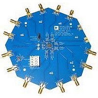
BOARD EVALUATION FOR ADCLK950
Manufacturer
Analog Devices Inc
Series
SIGer
Specifications of ADCLK950/PCBZ
Main Purpose
Timing, Clock Buffer / Driver / Receiver / Translator
Utilized Ic / Part
ADCLK950
Primary Attributes
2 Selectable Inputs, 10 Outputs
Secondary Attributes
LVPECL Output Logic
Silicon Manufacturer
Analog Devices
Application Sub Type
Clock Fanout Buffer
Kit Application Type
Clock & Timing
Silicon Core Number
ADCLK950
Lead Free Status / RoHS Status
Lead free / RoHS Compliant
Embedded
-
Lead Free Status / RoHS Status
Lead free / RoHS Compliant


SPECIFICATIONS
ELECTRICAL CHARACTERISTICS
Typical (Typ column) values are given for V
(Max column) values are given over the full V
Table 1. Clock Inputs and Outputs
Parameter
DC INPUT CHARACTERISTICS
DC OUTPUT CHARACTERISTICS
Table 2. Timing Characteristics
Parameter
AC PERFORMANCE
CLOCK OUTPUT PHASE NOISE
1
2
3
The output skew is the difference between any two similar delay paths while operating at the same voltage and temperature.
Measured at the rising edge of the clock signal; calculated using the SNR of the ADC method.
This is the amount of added jitter measured at the output while two related, asynchronous, differential frequencies are applied to the inputs.
Input Common Mode Voltage
Input Differential Range
Input Capacitance
Input Resistance
Input Bias Current
Hysteresis
Output Voltage High Level
Output Voltage Low Level
Output Voltage, Single Ended
Reference Voltage
Maximum Output Frequency
Output Rise Time
Output Fall Time
Propagation Delay
Output-to-Output Skew
Part-to-Part Skew
Additive Time Jitter
Absolute Phase Noise
Single-Ended Mode
Differential Mode
Common Mode
Output Voltage
Output Resistance
Temperature Coefficient
Integrated Random Jitter
Broadband Random Jitter
Crosstalk-Induced Jitter
f
IN
= 1 GHz
1
3
2
Symbol
Symbol
t
t
V
V
C
V
V
V
V
t
R
F
PD
ICM
ID
IN
OH
OL
O
REF
CC
− V
Min
V
0.4
V
V
610
Min
4.5
40
40
175
CC
EE
CC
CC
EE
− V
+ 1.5
− 1.26
− 1.99
= 3.3 V and T
EE
= 3.3 V ± 10% and T
Typ
0.4
50
100
50
20
10
(V
235
Typ
4.8
75
75
210
50
9
28
75
90
−119
−134
−145
−150
−150
CC
Rev. A | Page 3 of 12
A
+ 1)/2
= 25°C, unless otherwise noted. Minimum (Min column) and maximum
Max
V
3.4
V
V
960
Max
90
90
245
28
45
CC
CC
CC
A
− 0.1
− 0.76
− 1.54
= −40°C to +85°C variation, unless otherwise noted.
Unit
GHz
ps
ps
ps
fs/°C
ps
ps
fs rms
fs rms
fs rms
dBc/Hz
dBc/Hz
dBc/Hz
dBc/Hz
dBc/Hz
Unit
V
V p-p
pF
Ω
Ω
kΩ
μA
mV
V
V
mV
V
Ω
Test Conditions/Comments
±1.7 V between input pins
Open V
50 Ω to (V
50 Ω to (V
V
−500 μA to +500 μA
Test Conditions/Comments
See Figure 4 for differential output voltage vs.
frequency, >0.8 V differential output swing
20% to 80% measured differentially
V
V
BW = 12 kHz − 20 MHz, CLK = 1 GHz
V
Input slew rate > 1 V/ns (see Figure 11, the
phase noise plot, for more details)
@100 Hz offset
@1 kHz offset
@10 kHz offset
@100 kHz offset
>1 MHz offset
OH
ICM
ID
ID
= 1.6 V p-p
= 1.6 V p-p, 8 V/ns, V
− V
= 2 V, V
OL
T
x
, output static
CC
CC
ID
− 2.0 V)
− 2.0 V)
= 1.6 V p-p
ICM
= 2 V
ADCLK950
Related parts for ADCLK950/PCBZ
Image
Part Number
Description
Manufacturer
Datasheet
Request
R

Part Number:
Description:
±1.7g Dual-Axis IMEMS Accelerometer Evaluation Board
Manufacturer:
Analog Devices Inc
Datasheet:

Part Number:
Description:
Inertial Sensor Evaluation System
Manufacturer:
Analog Devices Inc
Datasheet:
Part Number:
Description:
Manufacturer:
Analog Devices Inc
Datasheet:
Part Number:
Description:
Manufacturer:
Analog Devices Inc
Datasheet:
Part Number:
Description:
Manufacturer:
Analog Devices Inc
Datasheet:
Part Number:
Description:
Manufacturer:
Analog Devices Inc
Datasheet:
Part Number:
Description:
Manufacturer:
Analog Devices Inc
Datasheet:
Part Number:
Description:
Manufacturer:
Analog Devices Inc
Datasheet:
Part Number:
Description:
Manufacturer:
Analog Devices Inc
Datasheet:
Part Number:
Description:
Manufacturer:
Analog Devices Inc
Datasheet:
Part Number:
Description:
Manufacturer:
Analog Devices Inc
Datasheet:
Part Number:
Description:
Manufacturer:
Analog Devices Inc
Datasheet:
Part Number:
Description:
Manufacturer:
Analog Devices Inc
Datasheet: