ADCLK950/PCBZ Analog Devices Inc, ADCLK950/PCBZ Datasheet - Page 2
ADCLK950/PCBZ
Manufacturer Part Number
ADCLK950/PCBZ
Description
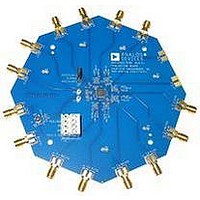
BOARD EVALUATION FOR ADCLK950
Manufacturer
Analog Devices Inc
Series
SIGer
Specifications of ADCLK950/PCBZ
Main Purpose
Timing, Clock Buffer / Driver / Receiver / Translator
Utilized Ic / Part
ADCLK950
Primary Attributes
2 Selectable Inputs, 10 Outputs
Secondary Attributes
LVPECL Output Logic
Silicon Manufacturer
Analog Devices
Application Sub Type
Clock Fanout Buffer
Kit Application Type
Clock & Timing
Silicon Core Number
ADCLK950
Lead Free Status / RoHS Status
Lead free / RoHS Compliant
Embedded
-
Lead Free Status / RoHS Status
Lead free / RoHS Compliant


ADCLK950
TABLE OF CONTENTS
Features .............................................................................................. 1
Applications ....................................................................................... 1
General Description ......................................................................... 1
Functional Block Diagram .............................................................. 1
Revision History ............................................................................... 2
Specifications ..................................................................................... 3
Absolute Maximum Ratings ............................................................ 5
REVISION HISTORY
6/10—Rev. 0 to Rev. A
Changed Output Voltage Differential Parameter to Output
Voltage, Single Ended Parameter, Table 1 ..................................... 3
Changes to Output Voltage, Single Ended Parameter, Table 1 ... 3
7/09—Revision 0: Initial Version
Electrical Characteristics ............................................................. 3
Determining Junction Temperature .......................................... 5
ESD Caution .................................................................................. 5
Thermal Performance .................................................................. 5
Rev. A | Page 2 of 12
Pin Configuration and Function Descriptions ..............................6
Typical Performance Characteristics ..............................................7
Functional Description .....................................................................9
Outline Dimensions ....................................................................... 12
Clock Inputs ...................................................................................9
Clock Outputs ................................................................................9
Clock Input Select (IN_SEL) Settings...................................... 10
PCB Layout Considerations ...................................................... 10
Input Termination Options ....................................................... 11
Ordering Guide .......................................................................... 12
Related parts for ADCLK950/PCBZ
Image
Part Number
Description
Manufacturer
Datasheet
Request
R

Part Number:
Description:
±1.7g Dual-Axis IMEMS Accelerometer Evaluation Board
Manufacturer:
Analog Devices Inc
Datasheet:

Part Number:
Description:
Inertial Sensor Evaluation System
Manufacturer:
Analog Devices Inc
Datasheet:
Part Number:
Description:
Manufacturer:
Analog Devices Inc
Datasheet:
Part Number:
Description:
Manufacturer:
Analog Devices Inc
Datasheet:
Part Number:
Description:
Manufacturer:
Analog Devices Inc
Datasheet:
Part Number:
Description:
Manufacturer:
Analog Devices Inc
Datasheet:
Part Number:
Description:
Manufacturer:
Analog Devices Inc
Datasheet:
Part Number:
Description:
Manufacturer:
Analog Devices Inc
Datasheet:
Part Number:
Description:
Manufacturer:
Analog Devices Inc
Datasheet:
Part Number:
Description:
Manufacturer:
Analog Devices Inc
Datasheet:
Part Number:
Description:
Manufacturer:
Analog Devices Inc
Datasheet:
Part Number:
Description:
Manufacturer:
Analog Devices Inc
Datasheet:
Part Number:
Description:
Manufacturer:
Analog Devices Inc
Datasheet: