AD9516-1/PCBZ Analog Devices Inc, AD9516-1/PCBZ Datasheet - Page 45
AD9516-1/PCBZ
Manufacturer Part Number
AD9516-1/PCBZ
Description
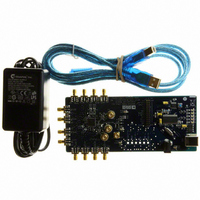
BOARD EVALUATION FOR AD9516-1
Manufacturer
Analog Devices Inc
Specifications of AD9516-1/PCBZ
Main Purpose
Timing, Clock Generator
Embedded
No
Utilized Ic / Part
AD9516-1
Primary Attributes
2 Inputs, 14 Outputs, 2.5GHz VCO
Secondary Attributes
CMOS, LVDS, LVPECL Output Logic, ADIsimCLK™ Graphical User Interface
Silicon Manufacturer
Analog Devices
Application Sub Type
PLL Clock Synthesizer
Kit Application Type
Clock & Timing
Silicon Core Number
AD9516-0, AD9516-1, AD9516-2
Silicon Family Name
AD9516-X
Rohs Compliant
Yes
Lead Free Status / RoHS Status
Lead free / RoHS Compliant


Table 44. Divider 3, Divider 4 Duty Cycle; VCO Divider Not
Used; Duty Cycle Correction On (DCCOFF = 0)
Input
Clock
Duty
Cycle
50%
50%
X%
X%
50%
X%
50%
X%
50%
X%
50%
X%
Phase Offset or Coarse Time Delay (Divider 3 and Divider 4)
Divider 3 and Divider 4 can be set to have a phase offset or
delay. The phase offset is set by a combination of the bits in the
phase offset and start high registers (see Table 45).
Table 45. Setting Phase Offset and Division for Divider 3 and
Divider 4
Divider
3
4
3.1
3.2
4.1
4.2
N
1
Even
(N
1
Even
(N
Odd
(M
Odd
(M
Odd
(M
Even
(N
Even
(N
Odd
(M
Odd
(M
Odd
(M
Odd
(M
X.1
X.1
X.1
X.1
X.1
Start
High (SH)
0x19C[0]
0x19C[1]
0x1A1[0]
0x1A1[1]
X.1
X.1
X.1
X.1
X.1
X.1
X.1
+ M
= M
= M
= N
= N
= N
= M
= M
= N
= N
= N
= N
D
X.1
X.1
X.1
X.1
X.1
X.1
X.1
X.1
X.1
X.1
X.1
X.1
X.1
+ 1)
+ 1)
+ 1)
+ 1)
+ 1)
+ 1)
+ 1)
)
)
)
)
+ 2
Phase
Offset (PO)
0x19A[3:0]
0x19A[7:4]
0x19F[3:0]
0x19F[7:4]
N
1
1
1
1
1
1
1
Even
(N
Even
(N
Even
(N
Even
(N
Odd
(M
Odd
(M
X.2
X.2
X.2
X.2
X.2
X.2
X.2
+ M
= M
= M
= M
= M
= N
= N
D
X.2
X.2
X.2
X.2
X.2
X.2
X.2
X.2
+ 1)
+ 1)
)
)
)
)
+ 2
Low
Cycles M
0x199[7:4]
0x19B[7:4]
0x1A0[7:4]
0x19E[7:4]
Output
Duty Cycle
50%
50%
X% (High)
50%
50%
(N
(2N
(N
(2N
50%
50%
50%
50%
50%
(2N
3N
((2N
X.1
X.1
X.2
X.1
X.1
X.1
X.1
+ 1 + X%)/
+ 1 + X%)/
+ 4 + X%)/
N
+ 3)
+ 3)
+ 3)(2N
X.2
+ 3N
High
Cycles N
0x199[3:0]
0x19B[3:0]
0x19E[3:0]
0x1A0[3:0]
X.2
X.1
+ 3))
+
Rev. A | Page 45 of 80
Let Δt = delay (in seconds).
Φ
1 × PO[0].
T
T
Case 1
When Φ
Δt = Φ
Case 2
When Φ
Δt = Φ
Case 3
When Φ
Δt = (Φ
Case 4
When Φ
Δt =
(Φ
Fine Delay Adjust (Divider 3 and Divider 4)
Each AD9516 LVDS/CMOS output (OUT6 to OUT9) includes
an analog delay element that can be programmed to give
variable time delays (Δt) in the clock signal at that output.
The amount of delay applied to the clock signal is determined
by programming four registers per output (see Table 46).
Table 46. Setting Analog Fine Delays
OUTPUT
(LVDS/CMOS)
OUT6
OUT7
OUT8
OUT9
CLK
X.1
X.2
x.y
X.1
= period of the clock signal at the input to D
= period of the clock signal at the input to D
= 16 × SH[0] + 8 × PO[3] + 4 × PO[2] + 2 × PO[1] +
DIVIDER
− 16 + M
VCO
x.1
X.1
X.1
DIVIDER
x.1
x.1
X.1
X.1
× T
× T
− 16 + M
X.1
≤ 15 and Φ
≤ 15 and Φ
≥ 16 and Φ
≥ 16 and Φ
X.1
X.1
X.1
+ Φ
+ (Φ
Ramp
Capacitors
0x0A1[5:3]
0x0A4[5:3]
0x0A7[5:3]
0x0AA[5:3]
Figure 56. Fine Delay (OUT6 to OUT9)
+ 1) × T
DIVIDER
X.2
X.1
X.2
X.2
× T
+ 1) × T
x.2
x.2
X.2
X.2
− 16 + M
≤ 15:
≥ 16:
≤ 15:
≥ 16:
x.2
X.1
+ (Φ
Ramp
Current
0x0A1[2:0]
0x0A4[2:0]
0x0A7[2:0]
0x0AA[2:0]
FINE DELAY
FINE DELAY
X.1
BYPASS
BYPASS
ADJUST
ADJUST
X.2
X.2
+ Φ
∆t
∆t
+ 1) × T
− 16 + M
X.2
× T
CMOS
CMOS
CMOS
CMOS
LVDS
LVDS
Delay
Fraction
0x0A2[5:0]
0x0A5[5:0]
0x0A8[5:0]
0x0AB[5:0]
X.2
X.2
X.2
+ 1) × T
AD9516-1
X.1
X.2
(in seconds).
(in seconds).
OUTPUT
DRIVERS
X.2
Delay
Bypass
0x0A0[0]
0x0A3[0]
0x0A6[0]
0x0A9[0]
OUTM
OUTM
OUTN
OUTN
Related parts for AD9516-1/PCBZ
Image
Part Number
Description
Manufacturer
Datasheet
Request
R

Part Number:
Description:
IC CLOCK PLL/VCO 2GHZ 64LFCSP
Manufacturer:
Analog Devices Inc
Datasheet:
Part Number:
Description:
IC CLOCK GEN 2.8GHZ VCO 64-LFCSP
Manufacturer:
Analog Devices Inc
Datasheet:
Part Number:
Description:
IC,Fourteen Distributed-Output Clock Driver,LLCC,64PIN,PLASTIC
Manufacturer:
Analog Devices Inc
Datasheet:
Part Number:
Description:
IC,Ten Distributed-Output Clock Driver,LLCC,64PIN,PLASTIC
Manufacturer:
Analog Devices Inc
Datasheet:
Part Number:
Description:
IC,Ten Distributed-Output Clock Driver,LLCC,64PIN,PLASTIC
Manufacturer:
Analog Devices Inc
Datasheet:
Part Number:
Description:
Clock IC With 1.8GHz On-chip VCO
Manufacturer:
Analog Devices Inc
Datasheet:

Part Number:
Description:
BOARD EVAL FOR AD9516-3 2.0GHZ
Manufacturer:
Analog Devices Inc
Datasheet:

Part Number:
Description:
BOARD EVAL FOR AD9516-4 1.8GHZ
Manufacturer:
Analog Devices Inc
Datasheet:
Part Number:
Description:
IC,Ten Distributed-Output Clock Driver,LLCC,64PIN,PLASTIC
Manufacturer:
Analog Devices Inc
Datasheet:
Part Number:
Description:
IC,Fourteen Distributed-Output Clock Driver,LLCC,64PIN,PLASTIC
Manufacturer:
Analog Devices Inc
Datasheet:
Part Number:
Description:
IC,Ten Distributed-Output Clock Driver,LLCC,64PIN,PLASTIC
Manufacturer:
Analog Devices Inc
Datasheet:
Part Number:
Description:
Clock IC With 1.8GHz On-chip VCO
Manufacturer:
Analog Devices Inc
Datasheet:
Part Number:
Description:
10/14 Chan Clock IC W/PLL-no VCO
Manufacturer:
Analog Devices Inc
Datasheet:
Part Number:
Description:
10/14 Chan Clock IC W/PLL-no VCO
Manufacturer:
Analog Devices Inc
Datasheet:

Part Number:
Description:
Clock IC With 2.5GHz On-chip VCO EB
Manufacturer:
Analog Devices Inc
Datasheet: