AD9516-1/PCBZ Analog Devices Inc, AD9516-1/PCBZ Datasheet - Page 37
AD9516-1/PCBZ
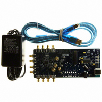
Manufacturer Part Number
AD9516-1/PCBZ
Description
BOARD EVALUATION FOR AD9516-1
Manufacturer
Analog Devices Inc
Specifications of AD9516-1/PCBZ
Main Purpose
Timing, Clock Generator
Embedded
No
Utilized Ic / Part
AD9516-1
Primary Attributes
2 Inputs, 14 Outputs, 2.5GHz VCO
Secondary Attributes
CMOS, LVDS, LVPECL Output Logic, ADIsimCLK™ Graphical User Interface
Silicon Manufacturer
Analog Devices
Application Sub Type
PLL Clock Synthesizer
Kit Application Type
Clock & Timing
Silicon Core Number
AD9516-0, AD9516-1, AD9516-2
Silicon Family Name
AD9516-X
Rohs Compliant
Yes
Lead Free Status / RoHS Status
Lead free / RoHS Compliant


Holdover
The AD9516 PLL has a holdover function. Holdover is
implemented by putting the charge pump into a state of high
impedance. This is useful when the PLL reference clock is lost.
Holdover mode allows the VCO to maintain a relatively constant
frequency even though there is no reference clock. Without this
function, the charge pump is placed into a constant pump-up or
pump-down state resulting in a massive VCO frequency shift.
Because the charge pump is placed in a high impedance state,
any leakage that occurs at the charge pump output or the VCO
tuning node causes a drift of the VCO frequency. This can be
mitigated by using a loop filter that contains a large capacitive
component because this drift is limited by the current leakage
induced slew rate (I
applications, the frequency accuracy is sufficient for 3 sec to 5 sec.
Both a manual holdover, using the SYNC pin, and an automatic
holdover mode are provided. To use either function, the
holdover function must be enabled (Register 0x01D[0] and
Register 0x01D[2]).
Note that the VCO cannot be calibrated with the holdover
enabled because the holdover resets the N divider during
calibration, which prevents proper calibration. Disable holdover
before issuing a VCO calibration.
Manual Holdover Mode
A manual holdover mode can be enabled that allows the user to
place the charge pump into a high impedance state when the
SYNC pin is asserted low. This operation is edge sensitive, not
level sensitive. The charge pump enters a high impedance state
immediately. To take the charge pump out of a high impedance
state take the SYNC pin high. The charge pump then leaves
high impedance state synchronously with the next PFD rising
edge from the reference clock. This prevents extraneous charge
pump events from occurring during the time between SYNC
going high and the next PFD event. This also means that the
charge pump stays in a high impedance state as long as there is
no reference clock present.
The B-counter (in the N divider) is reset synchronously with
the charge pump leaving the high impedance state on the
reference path PFD event. This helps align the edges out of the
R and N dividers for faster settling of the PLL. Because the
prescaler is not reset, this feature works best when the B and R
numbers are close because this results in a smaller phase
difference for the loop to settle out.
When using this mode, set the channel dividers to ignore the
SYNC pin (at least after an initial SYNC event). If the dividers are
not set to ignore the SYNC pin, the distribution outputs turn off
each time SYNC is taken low to put the part into holdover.
LEAK
/C) of the VCO control voltage. For most
Rev. A | Page 37 of 80
Automatic/Internal Holdover Mode
When enabled, this function automatically puts the charge
pump into a high impedance state when the loop loses lock.
The assumption is that the only reason the loop loses lock is due
to the PLL losing the reference clock; therefore, the holdover
function puts the charge pump into a high impedance state to
maintain the VCO frequency as close as possible to the original
frequency before the reference clock disappears.
See Figure 53 for a flowchart of the internal/automatic holdover
function operation.
HIGH IMPEDANCE
HIGH IMPEDANCE
WHEN DLD WENT
LD PIN == HIGH
CHARGE PUMP
CHARGE PUMP
EDGE AT PFD?
PLL ENABLED
DLD == LOW
DLD == HIGH
REFERENCE
RELEASE
LOW?
Figure 53. Flowchart of Automatic/Internal Holdover Mode
WAS
YES
YES
YES
YES
YES
NO
NO
NO
NO
YES
LOOP OUT OF LOCK. DIGITAL LOCK
DETECT SIGNAL GOES LOW WHEN THE
LOOP LEAVES LOCK AS DETERMINED
BY THE PHASE DIFFERENCE AT THE
INPUT OF THE PFD.
ANALOG LOCK DETECT PIN INDICATES
LOCK WAS PREVIOUSLY ACHIEVED.
REGISTER 0x1D[3] = 1: USE LD PIN
VOLTAGE WITH HOLDOVER.
REGISTER 0x1D[3] = 0: IGNORE LD PIN
VOLTAGE,TREAT LD PIN AS ALWAYS HIGH.
CHARGE PUMP IS MADE
HIGH IMPEDANCE.
PLL COUNTERS CONTINUE
OPERATING NORMALLY.
CHARGE PUMP REMAINS HIGH
IMPEDANCE UNTIL THE REFERENCE
HAS RETURNED.
TAKE CHARGE PUMP OUT OF
HIGH IMPEDANCE. PLL CAN
NOW RESETTLE.
WAIT FOR DLD TO GO HIGH. THIS TAKES
5 TO 255 CYCLES (PROGRAMMING OF
THE DLD DELAY COUNTER) WITH THE
REFERENCE AND FEEDBACK CLOCKS
INSIDE THE LOCK WINDOW AT THE PFD.
THIS ENSURES THAT THE HOLDOVER
FUNCTION WAITS FOR THE PLL TO SETTLE
AND LOCK BEFORE THE HOLDOVER
FUNCTION CAN BE RETRIGGERED.
AD9516-1
Related parts for AD9516-1/PCBZ
Image
Part Number
Description
Manufacturer
Datasheet
Request
R

Part Number:
Description:
IC CLOCK PLL/VCO 2GHZ 64LFCSP
Manufacturer:
Analog Devices Inc
Datasheet:
Part Number:
Description:
IC CLOCK GEN 2.8GHZ VCO 64-LFCSP
Manufacturer:
Analog Devices Inc
Datasheet:
Part Number:
Description:
IC,Fourteen Distributed-Output Clock Driver,LLCC,64PIN,PLASTIC
Manufacturer:
Analog Devices Inc
Datasheet:
Part Number:
Description:
IC,Ten Distributed-Output Clock Driver,LLCC,64PIN,PLASTIC
Manufacturer:
Analog Devices Inc
Datasheet:
Part Number:
Description:
IC,Ten Distributed-Output Clock Driver,LLCC,64PIN,PLASTIC
Manufacturer:
Analog Devices Inc
Datasheet:
Part Number:
Description:
Clock IC With 1.8GHz On-chip VCO
Manufacturer:
Analog Devices Inc
Datasheet:

Part Number:
Description:
BOARD EVAL FOR AD9516-3 2.0GHZ
Manufacturer:
Analog Devices Inc
Datasheet:

Part Number:
Description:
BOARD EVAL FOR AD9516-4 1.8GHZ
Manufacturer:
Analog Devices Inc
Datasheet:
Part Number:
Description:
IC,Ten Distributed-Output Clock Driver,LLCC,64PIN,PLASTIC
Manufacturer:
Analog Devices Inc
Datasheet:
Part Number:
Description:
IC,Fourteen Distributed-Output Clock Driver,LLCC,64PIN,PLASTIC
Manufacturer:
Analog Devices Inc
Datasheet:
Part Number:
Description:
IC,Ten Distributed-Output Clock Driver,LLCC,64PIN,PLASTIC
Manufacturer:
Analog Devices Inc
Datasheet:
Part Number:
Description:
Clock IC With 1.8GHz On-chip VCO
Manufacturer:
Analog Devices Inc
Datasheet:
Part Number:
Description:
10/14 Chan Clock IC W/PLL-no VCO
Manufacturer:
Analog Devices Inc
Datasheet:
Part Number:
Description:
10/14 Chan Clock IC W/PLL-no VCO
Manufacturer:
Analog Devices Inc
Datasheet:

Part Number:
Description:
Clock IC With 2.5GHz On-chip VCO EB
Manufacturer:
Analog Devices Inc
Datasheet: