AD9516-1/PCBZ Analog Devices Inc, AD9516-1/PCBZ Datasheet - Page 29
AD9516-1/PCBZ
Manufacturer Part Number
AD9516-1/PCBZ
Description
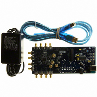
BOARD EVALUATION FOR AD9516-1
Manufacturer
Analog Devices Inc
Specifications of AD9516-1/PCBZ
Main Purpose
Timing, Clock Generator
Embedded
No
Utilized Ic / Part
AD9516-1
Primary Attributes
2 Inputs, 14 Outputs, 2.5GHz VCO
Secondary Attributes
CMOS, LVDS, LVPECL Output Logic, ADIsimCLK™ Graphical User Interface
Silicon Manufacturer
Analog Devices
Application Sub Type
PLL Clock Synthesizer
Kit Application Type
Clock & Timing
Silicon Core Number
AD9516-0, AD9516-1, AD9516-2
Silicon Family Name
AD9516-X
Rohs Compliant
Yes
Lead Free Status / RoHS Status
Lead free / RoHS Compliant


Internal VCO and Clock Distribution
When using the internal VCO and PLL, the VCO divider must
be employed to ensure that the frequency presented to the
channel dividers does not exceed their specified maximum
frequency of 1600 MHz (see Table 3). The internal PLL uses an
external loop filter to set the loop bandwidth. The external loop
filter is also crucial to the loop stability.
When using the internal VCO, it is necessary to calibrate the
VCO (Register 0x018[0]) to ensure optimal performance.
For internal VCO and clock distribution applications, use the
register settings that are shown in Table 24.
REFIN (REF1)
REFIN (REF2)
BYPASS
RESET
SYNC
SCLK
SDIO
SDO
CLK
CLK
PD
CS
LF
REF1
REF2
REGULATOR (LDO)
LOW DROPOUT
VCO
AD9516-1
CONTROL
DIGITAL
SWITCHOVER
SERIAL
STATUS
LOGIC
REFERENCE
PORT
REF_SEL
STATUS
VS
PRESCALER
2, 3, 4, 5, OR 6
1
P, P + 1
DIVIDE BY
GND
0
VCO STATUS
N DIVIDER
DIVIDER
Figure 44. Internal VCO and Clock Distribution
R
COUNTERS
DISTRIBUTION
DIVIDE BY
DIVIDE BY
REFERENCE
1 TO 32
1 TO 32
A/B
RSET
Rev. A | Page 29 of 80
DIVIDE BY
DIVIDE BY
DIVIDE BY
1 TO 32
1 TO 32
1 TO 32
PROGRAMMABLE
PROGRAMMABLE
R DELAY
N DELAY
REFMON
Table 24. Settings When Using Internal VCO
Register
0x010[1:0] = 00b
0x010 to 0x01E
0x018[0] = 0b,
0x232[0] = 1b
0x1E0[2:0]
0x1E1[0] = 0b
0x1E1[1] = 1b
0x018[0] = 1b,
0x232[0] = 1b
DIVIDE BY
DIVIDE BY
1 TO 32
1 TO 32
FREQUENCY
DETECTOR
DETECT
PHASE
LOCK
Function
PLL normal operation (PLL on).
PLL settings. Select and enable a reference
input; set R, N (P, A, B), PFD polarity, and I
according to the intended loop configuration.
Reset VCO calibration. This is not required
the first time after power-up, but it must
be performed subsequently.
Set VCO divider to divide-by-2, divide-by-3,
divide-by-4, divide-by-5, and divide-by-6.
Use the VCO divider as source for the
distribution section.
Select VCO as the source.
Initiate VCO calibration.
CPRSET VCP
∆
∆
∆
∆
t
t
t
t
CHARGE
PUMP
LVDS/CMOS
LVDS/CMOS
HOLD
LVPECL
LVPECL
LVPECL
OUT0
OUT0
OUT1
OUT1
OUT2
OUT2
OUT3
OUT3
OUT4
OUT4
OUT5
OUT5
OUT6 (OUT6A)
OUT6 (OUT6B)
OUT7 (OUT7A)
OUT7 (OUT7B)
OUT8 (OUT8A)
OUT8 (OUT8B)
OUT9 (OUT9A)
OUT9 (OUT9B)
LD
CP
STATUS
AD9516-1
CP
,
Related parts for AD9516-1/PCBZ
Image
Part Number
Description
Manufacturer
Datasheet
Request
R

Part Number:
Description:
IC CLOCK PLL/VCO 2GHZ 64LFCSP
Manufacturer:
Analog Devices Inc
Datasheet:
Part Number:
Description:
IC CLOCK GEN 2.8GHZ VCO 64-LFCSP
Manufacturer:
Analog Devices Inc
Datasheet:
Part Number:
Description:
IC,Fourteen Distributed-Output Clock Driver,LLCC,64PIN,PLASTIC
Manufacturer:
Analog Devices Inc
Datasheet:
Part Number:
Description:
IC,Ten Distributed-Output Clock Driver,LLCC,64PIN,PLASTIC
Manufacturer:
Analog Devices Inc
Datasheet:
Part Number:
Description:
IC,Ten Distributed-Output Clock Driver,LLCC,64PIN,PLASTIC
Manufacturer:
Analog Devices Inc
Datasheet:
Part Number:
Description:
Clock IC With 1.8GHz On-chip VCO
Manufacturer:
Analog Devices Inc
Datasheet:

Part Number:
Description:
BOARD EVAL FOR AD9516-3 2.0GHZ
Manufacturer:
Analog Devices Inc
Datasheet:

Part Number:
Description:
BOARD EVAL FOR AD9516-4 1.8GHZ
Manufacturer:
Analog Devices Inc
Datasheet:
Part Number:
Description:
IC,Ten Distributed-Output Clock Driver,LLCC,64PIN,PLASTIC
Manufacturer:
Analog Devices Inc
Datasheet:
Part Number:
Description:
IC,Fourteen Distributed-Output Clock Driver,LLCC,64PIN,PLASTIC
Manufacturer:
Analog Devices Inc
Datasheet:
Part Number:
Description:
IC,Ten Distributed-Output Clock Driver,LLCC,64PIN,PLASTIC
Manufacturer:
Analog Devices Inc
Datasheet:
Part Number:
Description:
Clock IC With 1.8GHz On-chip VCO
Manufacturer:
Analog Devices Inc
Datasheet:
Part Number:
Description:
10/14 Chan Clock IC W/PLL-no VCO
Manufacturer:
Analog Devices Inc
Datasheet:
Part Number:
Description:
10/14 Chan Clock IC W/PLL-no VCO
Manufacturer:
Analog Devices Inc
Datasheet:

Part Number:
Description:
Clock IC With 2.5GHz On-chip VCO EB
Manufacturer:
Analog Devices Inc
Datasheet: