AD9516-1/PCBZ Analog Devices Inc, AD9516-1/PCBZ Datasheet - Page 2
AD9516-1/PCBZ
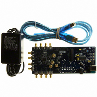
Manufacturer Part Number
AD9516-1/PCBZ
Description
BOARD EVALUATION FOR AD9516-1
Manufacturer
Analog Devices Inc
Specifications of AD9516-1/PCBZ
Main Purpose
Timing, Clock Generator
Embedded
No
Utilized Ic / Part
AD9516-1
Primary Attributes
2 Inputs, 14 Outputs, 2.5GHz VCO
Secondary Attributes
CMOS, LVDS, LVPECL Output Logic, ADIsimCLK™ Graphical User Interface
Silicon Manufacturer
Analog Devices
Application Sub Type
PLL Clock Synthesizer
Kit Application Type
Clock & Timing
Silicon Core Number
AD9516-0, AD9516-1, AD9516-2
Silicon Family Name
AD9516-X
Rohs Compliant
Yes
Lead Free Status / RoHS Status
Lead free / RoHS Compliant


AD9516-1
TABLE OF CONTENTS
Features .............................................................................................. 1
Applications....................................................................................... 1
General Description ......................................................................... 1
Functional Block Diagram .............................................................. 1
Revision History ............................................................................... 3
Specifications..................................................................................... 4
Timing Diagrams............................................................................ 15
Absolute Maximum Ratings.......................................................... 16
Power Supply Requirements ....................................................... 4
PLL Characteristics ...................................................................... 4
Clock Inputs .................................................................................. 6
Clock Outputs ............................................................................... 6
Timing Characteristics ................................................................ 7
Clock Output Additive Phase Noise (Distribution Only;
VCO Divider Not Used) .............................................................. 8
Clock Output Absolute Phase Noise (Internal VCO Used).... 9
Clock Output Absolute Time Jitter (Clock Generation
Using Internal VCO).................................................................. 10
Clock Output Absolute Time Jitter (Clock Cleanup
Using Internal VCO).................................................................. 10
Clock Output Absolute Time Jitter (Clock Generation
Using External VCXO) .............................................................. 10
Clock Output Additive Time Jitter (VCO Divider
Not Used)..................................................................................... 11
Clock Output Additive Time Jitter (VCO Divider Used) ..... 11
Delay Block Additive Time Jitter.............................................. 12
Serial Control Port ..................................................................... 12
PD , SYNC , and RESET Pins ..................................................... 13
LD, STATUS, and REFMON Pins............................................ 13
Power Dissipation....................................................................... 14
Rev. A | Page 2 of 80
Pin Configuration and Function Descriptions........................... 17
Typical Performance Characteristics ........................................... 19
Terminology .................................................................................... 25
Detailed Block Diagram ................................................................ 26
Theory of Operation ...................................................................... 27
Serial Control Port ......................................................................... 50
Thermal Performance.................................................................... 54
Register Map Overview ................................................................. 55
Register Map Descriptions ............................................................ 59
Applications Information .............................................................. 77
Outline Dimensions ....................................................................... 80
Thermal Resistance .................................................................... 16
ESD Caution................................................................................ 16
Operational Configurations...................................................... 27
Digital Lock Detect (DLD) ....................................................... 36
Clock Distribution ..................................................................... 40
Reset Modes ................................................................................ 48
Power-Down Modes .................................................................. 49
Serial Control Port Pin Descriptions....................................... 50
General Operation of Serial Control Port............................... 50
The Instruction Word (16 Bits) ................................................ 51
MSB/LSB First Transfers ........................................................... 51
Frequency Planning Using the AD9516.................................. 77
Using the AD9516 Outputs for ADC Clock Applications.... 77
LVPECL Clock Distribution ..................................................... 78
LVDS Clock Distribution .......................................................... 78
CMOS Clock Distribution ........................................................ 79
Ordering Guide .......................................................................... 80
Related parts for AD9516-1/PCBZ
Image
Part Number
Description
Manufacturer
Datasheet
Request
R

Part Number:
Description:
IC CLOCK PLL/VCO 2GHZ 64LFCSP
Manufacturer:
Analog Devices Inc
Datasheet:
Part Number:
Description:
IC CLOCK GEN 2.8GHZ VCO 64-LFCSP
Manufacturer:
Analog Devices Inc
Datasheet:
Part Number:
Description:
IC,Fourteen Distributed-Output Clock Driver,LLCC,64PIN,PLASTIC
Manufacturer:
Analog Devices Inc
Datasheet:
Part Number:
Description:
IC,Ten Distributed-Output Clock Driver,LLCC,64PIN,PLASTIC
Manufacturer:
Analog Devices Inc
Datasheet:
Part Number:
Description:
IC,Ten Distributed-Output Clock Driver,LLCC,64PIN,PLASTIC
Manufacturer:
Analog Devices Inc
Datasheet:
Part Number:
Description:
Clock IC With 1.8GHz On-chip VCO
Manufacturer:
Analog Devices Inc
Datasheet:

Part Number:
Description:
BOARD EVAL FOR AD9516-3 2.0GHZ
Manufacturer:
Analog Devices Inc
Datasheet:

Part Number:
Description:
BOARD EVAL FOR AD9516-4 1.8GHZ
Manufacturer:
Analog Devices Inc
Datasheet:
Part Number:
Description:
IC,Ten Distributed-Output Clock Driver,LLCC,64PIN,PLASTIC
Manufacturer:
Analog Devices Inc
Datasheet:
Part Number:
Description:
IC,Fourteen Distributed-Output Clock Driver,LLCC,64PIN,PLASTIC
Manufacturer:
Analog Devices Inc
Datasheet:
Part Number:
Description:
IC,Ten Distributed-Output Clock Driver,LLCC,64PIN,PLASTIC
Manufacturer:
Analog Devices Inc
Datasheet:
Part Number:
Description:
Clock IC With 1.8GHz On-chip VCO
Manufacturer:
Analog Devices Inc
Datasheet:
Part Number:
Description:
10/14 Chan Clock IC W/PLL-no VCO
Manufacturer:
Analog Devices Inc
Datasheet:
Part Number:
Description:
10/14 Chan Clock IC W/PLL-no VCO
Manufacturer:
Analog Devices Inc
Datasheet:

Part Number:
Description:
Clock IC With 2.5GHz On-chip VCO EB
Manufacturer:
Analog Devices Inc
Datasheet: