AD9516-1/PCBZ Analog Devices Inc, AD9516-1/PCBZ Datasheet - Page 33
AD9516-1/PCBZ
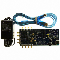
Manufacturer Part Number
AD9516-1/PCBZ
Description
BOARD EVALUATION FOR AD9516-1
Manufacturer
Analog Devices Inc
Specifications of AD9516-1/PCBZ
Main Purpose
Timing, Clock Generator
Embedded
No
Utilized Ic / Part
AD9516-1
Primary Attributes
2 Inputs, 14 Outputs, 2.5GHz VCO
Secondary Attributes
CMOS, LVDS, LVPECL Output Logic, ADIsimCLK™ Graphical User Interface
Silicon Manufacturer
Analog Devices
Application Sub Type
PLL Clock Synthesizer
Kit Application Type
Clock & Timing
Silicon Core Number
AD9516-0, AD9516-1, AD9516-2
Silicon Family Name
AD9516-X
Rohs Compliant
Yes
Lead Free Status / RoHS Status
Lead free / RoHS Compliant


Charge Pump (CP)
The charge pump is controlled by the PFD. The PFD monitors
the phase and frequency relationship between its two inputs,
and tells the CP to pump up or pump down to charge or discharge
the integrating node (part of the loop filter). The integrated and
filtered CP current is transformed into a voltage that drives the
tuning node of the internal VCO through the LF pin (or the tuning
pin of an external VCO) to move the VCO frequency up or down.
The CP can be set (Register 0x010[6:4]) for high impedance
(allows holdover operation), for normal operation (attempts to
lock the PLL loop), for pump up, or for pump down (test modes).
The CP current is programmable in eight steps from (nominally)
600 μA to 4.8 mA. The exact value of the CP current LSB is set
by the CPRSET resistor, which is nominally 5.1 kΩ. If the value
of the resistor connected to the CP_RSET pin is doubled, the
resulting charge pump current range becomes 300 μA to 2.4 mA.
On-Chip VCO
The AD9516 includes an on-chip VCO covering the frequency
range shown in Table 2. The calibration procedure ensures that
the VCO operating voltage is centered for the desired VCO
frequency. The VCO must be calibrated when the VCO loop is first
set up, as well as any time the nominal VCO frequency changes.
However, once the VCO is calibrated, the VCO has sufficient
operating range to stay locked over temperature and voltage
extremes without needing additional calibration. See the VCO
Calibration section for more information.
The on-chip VCO is powered by an on-chip, low dropout
(LDO), linear voltage regulator. The LDO provides some
isolation of the VCO from variations in the power supply
voltage level. The BYPASS pin should be connected to ground
by a 220 nF capacitor to ensure stability. This LDO employs the
same technology used in the anyCAP® line of regulators from
Analog Devices, Inc., making it insensitive to the type of
capacitor used. Driving an external load from the BYPASS pin
is not supported.
Note that the reference input signal must be present and the
VCO divider must not be static during VCO calibration.
PLL External Loop Filter
When using the internal VCO, the external loop filter should
be referenced to the BYPASS pin for optimal noise and spurious
performance. An example of an external loop filter for a PLL
that uses the internal VCO is shown in Figure 47. The third-
order design shown in Figure 47 usually offers best performance.
A loop filter must be calculated for each desired PLL configuration.
The values of the components depend upon the VCO frequency,
the K
bandwidth, and the desired phase margin. The loop filter affects
the phase noise, the loop settling time, and loop stability. A basic
knowledge of PLL theory is helpful for understanding loop filter
design. ADIsimCLK can help with calculation of a loop filter
according to application requirements.
VCO
, the PFD frequency, the CP current, the desired loop
Rev. A | Page 33 of 80
When using an external VCO, the external loop filter should be
referenced to ground. See Figure 48 for an example of an
external loop filter for a PLL using an external VCO.
PLL Reference Inputs
The AD9516 features a flexible PLL reference input circuit that
allows either a fully differential input or two separate single-
ended inputs. The input frequency range for the reference
inputs is specified in Table 2. Both the differential and the
single-ended inputs are self-biased, allowing for easy ac
coupling of input signals.
The differential input and the single-ended inputs share the two
pins, REFIN/ REFIN (REF1 and REF2, respectively). The desired
reference input type is selected and controlled by Register 0x01C
(see
When the differential reference input is selected, the self-bias
level of the two sides is offset slightly (~100 mV, see Table 2) to
prevent chattering of the input buffer when the reference is slow
or missing. This increases the voltage swing that is required of the
driver and overcomes the offset. The differential reference input
can be driven by either ac-coupled LVDS or ac-coupled LVPECL
signals.
The single-ended inputs can be driven by either a dc-coupled
CMOS level signal or an ac-coupled sine wave or square wave.
Each single-ended input can be independently powered down
when not needed to increase isolation and reduce power. Either
a differential or a single-ended reference must be specifically
enabled. All PLL reference inputs are off by default.
The differential reference input is powered down whenever the
PLL is powered down, or when the differential reference input
is not selected. The single-ended buffers power down when the
PLL is powered down, and when their individual power down
registers are set. When the differential mode is selected, the
single-ended inputs are powered down.
Figure 47. Example of External Loop Filter for a PLL Using the Internal VCO
Figure 48. Example of External Loop Filter for a PLL Using an External VCO
Table 52
and
AD9516-1
AD9516-1
CHARGE
CHARGE
PUMP
PUMP
Table 54
VCO
31pF
).
LF
CP
BYPASS
CLK/CLK
CP
C
BP
= 220nF
C1
C1
EXTERNAL
VCO/VCXO
R1
R1
C2
C2
R2
R2
C3
C3
AD9516-1
Related parts for AD9516-1/PCBZ
Image
Part Number
Description
Manufacturer
Datasheet
Request
R

Part Number:
Description:
IC CLOCK PLL/VCO 2GHZ 64LFCSP
Manufacturer:
Analog Devices Inc
Datasheet:
Part Number:
Description:
IC CLOCK GEN 2.8GHZ VCO 64-LFCSP
Manufacturer:
Analog Devices Inc
Datasheet:
Part Number:
Description:
IC,Fourteen Distributed-Output Clock Driver,LLCC,64PIN,PLASTIC
Manufacturer:
Analog Devices Inc
Datasheet:
Part Number:
Description:
IC,Ten Distributed-Output Clock Driver,LLCC,64PIN,PLASTIC
Manufacturer:
Analog Devices Inc
Datasheet:
Part Number:
Description:
IC,Ten Distributed-Output Clock Driver,LLCC,64PIN,PLASTIC
Manufacturer:
Analog Devices Inc
Datasheet:
Part Number:
Description:
Clock IC With 1.8GHz On-chip VCO
Manufacturer:
Analog Devices Inc
Datasheet:

Part Number:
Description:
BOARD EVAL FOR AD9516-3 2.0GHZ
Manufacturer:
Analog Devices Inc
Datasheet:

Part Number:
Description:
BOARD EVAL FOR AD9516-4 1.8GHZ
Manufacturer:
Analog Devices Inc
Datasheet:
Part Number:
Description:
IC,Ten Distributed-Output Clock Driver,LLCC,64PIN,PLASTIC
Manufacturer:
Analog Devices Inc
Datasheet:
Part Number:
Description:
IC,Fourteen Distributed-Output Clock Driver,LLCC,64PIN,PLASTIC
Manufacturer:
Analog Devices Inc
Datasheet:
Part Number:
Description:
IC,Ten Distributed-Output Clock Driver,LLCC,64PIN,PLASTIC
Manufacturer:
Analog Devices Inc
Datasheet:
Part Number:
Description:
Clock IC With 1.8GHz On-chip VCO
Manufacturer:
Analog Devices Inc
Datasheet:
Part Number:
Description:
10/14 Chan Clock IC W/PLL-no VCO
Manufacturer:
Analog Devices Inc
Datasheet:
Part Number:
Description:
10/14 Chan Clock IC W/PLL-no VCO
Manufacturer:
Analog Devices Inc
Datasheet:

Part Number:
Description:
Clock IC With 2.5GHz On-chip VCO EB
Manufacturer:
Analog Devices Inc
Datasheet: