OM6290 NXP Semiconductors, OM6290 Datasheet - Page 39
OM6290
Manufacturer Part Number
OM6290
Description
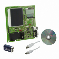
DEMO BOARD LCD GRAPHIC DRIVER
Manufacturer
NXP Semiconductors
Datasheets
1.PCF8576T1118.pdf
(44 pages)
2.OM6290.pdf
(30 pages)
3.OM6290.pdf
(51 pages)
4.OM6290.pdf
(83 pages)
Specifications of OM6290
Main Purpose
Displays, LCD Controller
Embedded
Yes, MCU, 16/32-Bit
Utilized Ic / Part
PCF2119, PCF8531, PCF8576
Primary Attributes
Character, Graphic and Segment LCD Drivers
Secondary Attributes
JTAG, I²C, UART & USB Interfaces
Description/function
Demo Board
Interface Type
USB, I2C, JTAG, UART
Data Bus Width
4 bit, 8 bit, 16 bit
Operating Voltage
1.8 V to 5.5 V
For Use With/related Products
PCF8576DT, PCF2119S, PCF8531
Lead Free Status / RoHS Status
Lead free / RoHS Compliant
Lead Free Status / RoHS Status
Lead free / RoHS Compliant, Lead free / RoHS Compliant
Other names
568-4703


Philips Semiconductors
17 SOLDERING
17.1
This text gives a very brief insight to a complex technology.
A more in-depth account of soldering ICs can be found in
our “Data Handbook IC26; Integrated Circuit Packages”
(document order number 9398 652 90011).
There is no soldering method that is ideal for all surface
mount IC packages. Wave soldering can still be used for
certain surface mount ICs, but it is not suitable for fine pitch
SMDs. In these situations reflow soldering is
recommended.
17.2
Reflow soldering requires solder paste (a suspension of
fine solder particles, flux and binding agent) to be applied
to the printed-circuit board by screen printing, stencilling or
pressure-syringe dispensing before package placement.
Several methods exist for reflowing; for example,
convection or convection/infrared heating in a conveyor
type oven. Throughput times (preheating, soldering and
cooling) vary between 100 and 200 seconds depending
on heating method.
Typical reflow peak temperatures range from
215 to 250 C. The top-surface temperature of the
packages should preferable be kept below 220 C for
thick/large packages, and below 235 C for small/thin
packages.
17.3
Conventional single wave soldering is not recommended
for surface mount devices (SMDs) or printed-circuit boards
with a high component density, as solder bridging and
non-wetting can present major problems.
To overcome these problems the double-wave soldering
method was specifically developed.
2001 Oct 02
Universal LCD driver for low multiplex rates
Introduction to soldering surface mount
packages
Reflow soldering
Wave soldering
39
If wave soldering is used the following conditions must be
observed for optimal results:
During placement and before soldering, the package must
be fixed with a droplet of adhesive. The adhesive can be
applied by screen printing, pin transfer or syringe
dispensing. The package can be soldered after the
adhesive is cured.
Typical dwell time is 4 seconds at 250 C.
A mildly-activated flux will eliminate the need for removal
of corrosive residues in most applications.
17.4
Fix the component by first soldering two
diagonally-opposite end leads. Use a low voltage (24 V or
less) soldering iron applied to the flat part of the lead.
Contact time must be limited to 10 seconds at up to
300 C.
When using a dedicated tool, all other leads can be
soldered in one operation within 2 to 5 seconds between
270 and 320 C.
Use a double-wave soldering method comprising a
turbulent wave with high upward pressure followed by a
smooth laminar wave.
For packages with leads on two sides and a pitch (e):
– larger than or equal to 1.27 mm, the footprint
– smaller than 1.27 mm, the footprint longitudinal axis
The footprint must incorporate solder thieves at the
downstream end.
For packages with leads on four sides, the footprint must
be placed at a 45 angle to the transport direction of the
printed-circuit board. The footprint must incorporate
solder thieves downstream and at the side corners.
longitudinal axis is preferred to be parallel to the
transport direction of the printed-circuit board;
must be parallel to the transport direction of the
printed-circuit board.
Manual soldering
Product specification
PCF8576
Related parts for OM6290
Image
Part Number
Description
Manufacturer
Datasheet
Request
R

Part Number:
Description:
NXP Semiconductors designed the LPC2420/2460 microcontroller around a 16-bit/32-bitARM7TDMI-S CPU core with real-time debug interfaces that include both JTAG andembedded trace
Manufacturer:
NXP Semiconductors
Datasheet:

Part Number:
Description:
NXP Semiconductors designed the LPC2458 microcontroller around a 16-bit/32-bitARM7TDMI-S CPU core with real-time debug interfaces that include both JTAG andembedded trace
Manufacturer:
NXP Semiconductors
Datasheet:
Part Number:
Description:
NXP Semiconductors designed the LPC2468 microcontroller around a 16-bit/32-bitARM7TDMI-S CPU core with real-time debug interfaces that include both JTAG andembedded trace
Manufacturer:
NXP Semiconductors
Datasheet:
Part Number:
Description:
NXP Semiconductors designed the LPC2470 microcontroller, powered by theARM7TDMI-S core, to be a highly integrated microcontroller for a wide range ofapplications that require advanced communications and high quality graphic displays
Manufacturer:
NXP Semiconductors
Datasheet:
Part Number:
Description:
NXP Semiconductors designed the LPC2478 microcontroller, powered by theARM7TDMI-S core, to be a highly integrated microcontroller for a wide range ofapplications that require advanced communications and high quality graphic displays
Manufacturer:
NXP Semiconductors
Datasheet:
Part Number:
Description:
The Philips Semiconductors XA (eXtended Architecture) family of 16-bit single-chip microcontrollers is powerful enough to easily handle the requirements of high performance embedded applications, yet inexpensive enough to compete in the market for hi
Manufacturer:
NXP Semiconductors
Datasheet:
Part Number:
Description:
The XA-S3 device is a member of Philips Semiconductors? XA(eXtended Architecture) family of high performance 16-bitsingle-chip microcontrollers
Manufacturer:
NXP Semiconductors
Datasheet:

Part Number:
Description:
The NXP BlueStreak LH75401/LH75411 family consists of two low-cost 16/32-bit System-on-Chip (SoC) devices
Manufacturer:
NXP Semiconductors
Datasheet:
Part Number:
Description:
The NXP LPC3130/3131 combine an 180 MHz ARM926EJ-S CPU core, high-speed USB2
Manufacturer:
NXP Semiconductors
Datasheet:
Part Number:
Description:
The NXP LPC3141 combine a 270 MHz ARM926EJ-S CPU core, High-speed USB 2
Manufacturer:
NXP Semiconductors
Part Number:
Description:
The NXP LPC3143 combine a 270 MHz ARM926EJ-S CPU core, High-speed USB 2
Manufacturer:
NXP Semiconductors

Part Number:
Description:
The NXP LPC3152 combines an 180 MHz ARM926EJ-S CPU core, High-speed USB 2
Manufacturer:
NXP Semiconductors
Part Number:
Description:
The NXP LPC3154 combines an 180 MHz ARM926EJ-S CPU core, High-speed USB 2
Manufacturer:
NXP Semiconductors

Part Number:
Description:
Standard level N-channel enhancement mode Field-Effect Transistor (FET) in a plastic package using NXP High-Performance Automotive (HPA) TrenchMOS technology
Manufacturer:
NXP Semiconductors
Datasheet: