OM6290 NXP Semiconductors, OM6290 Datasheet - Page 28
OM6290
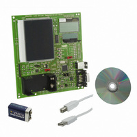
Manufacturer Part Number
OM6290
Description
DEMO BOARD LCD GRAPHIC DRIVER
Manufacturer
NXP Semiconductors
Datasheets
1.PCF8576T1118.pdf
(44 pages)
2.OM6290.pdf
(30 pages)
3.OM6290.pdf
(51 pages)
4.OM6290.pdf
(83 pages)
Specifications of OM6290
Main Purpose
Displays, LCD Controller
Embedded
Yes, MCU, 16/32-Bit
Utilized Ic / Part
PCF2119, PCF8531, PCF8576
Primary Attributes
Character, Graphic and Segment LCD Drivers
Secondary Attributes
JTAG, I²C, UART & USB Interfaces
Description/function
Demo Board
Interface Type
USB, I2C, JTAG, UART
Data Bus Width
4 bit, 8 bit, 16 bit
Operating Voltage
1.8 V to 5.5 V
For Use With/related Products
PCF8576DT, PCF2119S, PCF8531
Lead Free Status / RoHS Status
Lead free / RoHS Compliant
Lead Free Status / RoHS Status
Lead free / RoHS Compliant, Lead free / RoHS Compliant
Other names
568-4703


Philips Semiconductors
10 DC CHARACTERISTICS
V
Notes
1. V
2. LCD outputs are open-circuit; inputs at V
3. Resets all logic when V
4. Periodically sampled, not 100% tested.
5. Outputs measured one at a time.
2001 Oct 02
Supplies
V
V
I
Logic
V
V
V
V
I
I
I
I
I
I
R
V
C
LCD outputs
V
V
R
R
SYMBOL
DD
OL1
OH1
OL2
L1
L2
pd
DD
DD
LCD
IL
IH
OL
OH
POR
BP
S
SYNC
I
BP
S
Universal LCD driver for low multiplex rates
= 2 to 9 V; V
LCD
V
supply voltage
LCD supply voltage
supply current
LOW-level input voltage
HIGH-level input voltage
LOW-level output voltage
HIGH-level output voltage
LOW-level output current
CLK, SYNC
HIGH-level output current CLK
LOW-level output current
SDA and SCL
leakage current SA0, A0 to A2,
CLK, SDA and SCL
leakage current OSC
A0, A1, A2 and OSC pull-down
current
pull-up resistor (SYNC)
Power-on reset voltage level
input capacitance
DC voltage component BP0 to BP3
DC voltage component S0 to S39
output resistance BP0 to BP3
output resistance S0 to S39
DD
normal mode
power-saving mode
SS
3 V for
= 0 V; V
PARAMETER
1
3
bias.
DD
LCD
< V
= V
POR
DD
.
2 V to V
SS
or V
DD
note 1
note 2
f
f
V
connected to V
I
I
V
V
V
V
V
V
note 3
note 4
C
C
note 5; V
note 5; V
clk
clk
OL
OH
DD
LCD
OL
OH
OL
I
I
I
BP
S
9 V; T
= 1 V; V
= V
= V
= 200 kHz
= 35 kHz; V
; external clock with 50% duty factor; I
= 5 nF
= 0 mA
= 0 mA
= 1 V; V
= 0.4 V; V
= 35 nF
= 4 V; V
= 0 V; A0, A1 and A2
DD
DD
CONDITIONS
28
amb
or V
LCD
LCD
DD
= 40 to +85 C; unless otherwise specified.
DD
DD
= V
= V
SS
= 5 V
DD
DD
SS
= 5 V
= 5 V
DD
DD
= 5 V
= 3.5 V;
5 V
5 V
2
V
V
0.7V
V
1
1
3
20
20
DD
SS
DD
MIN.
DD
9
0.05
2
50
50
1.0
20
20
C-bus inactive.
TYP.
Product specification
9
V
180
60
0.3V
V
0.05
1
1
150
150
1.6
7
5
7.5
PCF8576
MAX.
DD
DD
DD
2 V
V
V
V
V
V
mA
mA
mA
k
V
pF
mV
mV
k
k
UNIT
A
A
A
A
A
Related parts for OM6290
Image
Part Number
Description
Manufacturer
Datasheet
Request
R

Part Number:
Description:
NXP Semiconductors designed the LPC2420/2460 microcontroller around a 16-bit/32-bitARM7TDMI-S CPU core with real-time debug interfaces that include both JTAG andembedded trace
Manufacturer:
NXP Semiconductors
Datasheet:

Part Number:
Description:
NXP Semiconductors designed the LPC2458 microcontroller around a 16-bit/32-bitARM7TDMI-S CPU core with real-time debug interfaces that include both JTAG andembedded trace
Manufacturer:
NXP Semiconductors
Datasheet:
Part Number:
Description:
NXP Semiconductors designed the LPC2468 microcontroller around a 16-bit/32-bitARM7TDMI-S CPU core with real-time debug interfaces that include both JTAG andembedded trace
Manufacturer:
NXP Semiconductors
Datasheet:
Part Number:
Description:
NXP Semiconductors designed the LPC2470 microcontroller, powered by theARM7TDMI-S core, to be a highly integrated microcontroller for a wide range ofapplications that require advanced communications and high quality graphic displays
Manufacturer:
NXP Semiconductors
Datasheet:
Part Number:
Description:
NXP Semiconductors designed the LPC2478 microcontroller, powered by theARM7TDMI-S core, to be a highly integrated microcontroller for a wide range ofapplications that require advanced communications and high quality graphic displays
Manufacturer:
NXP Semiconductors
Datasheet:
Part Number:
Description:
The Philips Semiconductors XA (eXtended Architecture) family of 16-bit single-chip microcontrollers is powerful enough to easily handle the requirements of high performance embedded applications, yet inexpensive enough to compete in the market for hi
Manufacturer:
NXP Semiconductors
Datasheet:
Part Number:
Description:
The XA-S3 device is a member of Philips Semiconductors? XA(eXtended Architecture) family of high performance 16-bitsingle-chip microcontrollers
Manufacturer:
NXP Semiconductors
Datasheet:

Part Number:
Description:
The NXP BlueStreak LH75401/LH75411 family consists of two low-cost 16/32-bit System-on-Chip (SoC) devices
Manufacturer:
NXP Semiconductors
Datasheet:
Part Number:
Description:
The NXP LPC3130/3131 combine an 180 MHz ARM926EJ-S CPU core, high-speed USB2
Manufacturer:
NXP Semiconductors
Datasheet:
Part Number:
Description:
The NXP LPC3141 combine a 270 MHz ARM926EJ-S CPU core, High-speed USB 2
Manufacturer:
NXP Semiconductors
Part Number:
Description:
The NXP LPC3143 combine a 270 MHz ARM926EJ-S CPU core, High-speed USB 2
Manufacturer:
NXP Semiconductors

Part Number:
Description:
The NXP LPC3152 combines an 180 MHz ARM926EJ-S CPU core, High-speed USB 2
Manufacturer:
NXP Semiconductors
Part Number:
Description:
The NXP LPC3154 combines an 180 MHz ARM926EJ-S CPU core, High-speed USB 2
Manufacturer:
NXP Semiconductors

Part Number:
Description:
Standard level N-channel enhancement mode Field-Effect Transistor (FET) in a plastic package using NXP High-Performance Automotive (HPA) TrenchMOS technology
Manufacturer:
NXP Semiconductors
Datasheet: