LTM4611EV#PBF Linear Technology, LTM4611EV#PBF Datasheet - Page 7
LTM4611EV#PBF
Manufacturer Part Number
LTM4611EV#PBF
Description
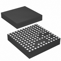
IC UMODULE DC/DC LV 15A 133-LGA
Manufacturer
Linear Technology
Series
µModuler
Type
Point of Load (POL) Non-Isolatedr
Datasheet
1.LTM4611EVPBF.pdf
(28 pages)
Specifications of LTM4611EV#PBF
Output
0.8 ~ 5 V
Number Of Outputs
1
Power (watts)
75W
Mounting Type
Surface Mount
Voltage - Input
1.5 ~ 5.5 V
Package / Case
133-LGA
1st Output
0.8 ~ 5 VDC @ 15A
Size / Dimension
0.59" L x 0.59" W x 0.17" H (15mm x 15mm x 4.32mm)
Power (watts) - Rated
75W
Operating Temperature
-40°C ~ 125°C
Efficiency
94%
Lead Free Status / RoHS Status
Lead free / RoHS Compliant
3rd Output
-
2nd Output
-
Available stocks
Company
Part Number
Manufacturer
Quantity
Price


Typical perForMance characTerisTics
pin FuncTions
V
voltage between these pins and GND pins. Recommend
placing input decoupling capacitance directly between
V
V
Pins. Apply output load between these pins and GND
pins. Recommend placing output decoupling capacitance
directly between these pins and GND pins. Review Table 5.
GND: (B7, B9, C7, C9, D1-D6, D8, E1-E7, E9, F1-F9, G1-G9,
H1-H9) Power Ground Pins for Both Input and Output
Returns.
PGOOD: (F11, G12) Output Voltage Power Good Indicator.
Open-drain logic output that is pulled to ground when the
output voltage exceeds a ±5% regulation window. Both
pins are tied together internally.
AC-COUPLED
IN
IN
OUT
500mV/DIV
50mV/DIV
2mA/DIV
: (A1-A6, B1-B6, C1-C6) Power Input Pins. Apply input
pins and GND pins.
5A/DIV
1A/DIV
5V/DIV
I
: (J1-J10, K1-K11, L1-L11, M1-M11) Power Output
I
V
V
LOAD
LOAD
RUN
OUT
OUT
I
IN
3.3V Transient Response, 5V
V
2 100µF CERAMIC OUTPUT CAPACITORS
C
7.5A LOAD STEP AT 7.5A/µs
V
3 22µF CERAMIC INPUT CAPACITORS
C
4 100µF CERAMIC OUTPUT CAPACITORS
C
Start-Up, Pre-Bias
IN
FF
IN
SS
FF
= 5V, V
= 10pF , C
= 3.3V, V
= 33pF , C
= 10nF
OUT
OUT
P
P
= NONE
= 10pF
= 3.3V, USING DIFF AMP
= 1.5V, 0.75V PRE-BIAS LOAD
20µs/DIV
2ms/DIV
IN
4611 G08
4611 G13
500mV/DIV
500mV/DIV
1V/DIV
1A/DIV
2A/DIV
V
V
OUT
OUT
V
I
I
IN
IN
IN
Start-Up, No Load
Short-Circuit, 15A
V
3 22µF CERAMIC INPUT CAPACITORS
C
4 100µF CERAMIC OUTPUT CAPACITORS
C
V
15A LOAD PRIOR TO SHORT
IN
SS
FF
IN
= 3.3V, V
= 33pF , C
= 3.3V, V
= 10nF
OUT
OUT
P
= 10pF
= 1.5V, NO LOAD
= 1.5V
20µs/DIV
1ms/DIV
SGND: (G11, H11, H12) Signal Ground Pin. Return ground
path for all analog and low power circuitry. Tie a single
connection to the output capacitor GND in the application.
See the layout guidelines in Figure 17.
MODE_PLLIN: (A8) Forced Continuous Mode, Burst Mode
Operation, or Pulse-Skipping Mode Selection Pin and
External Synchronization Input to Phase Detector Pin.
Connect this pin to GND to force continuous mode
operation. Connect to INTV
ping mode operation. Leaving the pin floating will
enable Burst Mode operation. A clock on this pin will
enable synchronization with forced continuous operation.
See the Applications Information section.
4611 G09
4611 G10
500mV/DIV
500mV/DIV
1V/DIV
5A/DIV
5A/DIV
1A/DIV
I
V
LOAD
V
OUT
OUT
V
I
I
IN
IN
IN
Start-Up, 15A Load
Short-Circuit, No Load
V
3 22µF CERAMIC INPUT CAPACITORS
C
4 100µF CERAMIC OUTPUT CAPACITORS
C
V
NO LOAD PRIOR TO SHORT
IN
SS
FF
IN
= 3.3V, V
= 33pF , C
= 3.3V, V
= 10nF
CC
to enable pulse-skip-
OUT
OUT
P
= 10pF
= 1.5V, 100m LOAD
= 1.5V
LTM4611
20µs/DIV
1ms/DIV
4611 G12
4611 G11
4611f
Related parts for LTM4611EV#PBF
Image
Part Number
Description
Manufacturer
Datasheet
Request
R

Part Number:
Description:
Ltm4611 Ultralow Vin, 15a Dc/dc ?module Regulator Features
Manufacturer:
Linear Technology Corporation
Datasheet:

Part Number:
Description:
CD ROM LINEARVIEW DATASHEETS
Manufacturer:
Linear Technology
Part Number:
Description:
Standalone Linear Li-Ion Battery Charger with Thermal Regulation in ThinSOT
Manufacturer:
Linear Technology Corporation
Datasheet:
Part Number:
Description:
Low noise, high frequency, 8th order linear phase lowpass filter
Manufacturer:
Linear Technology Corporation
Datasheet:
Part Number:
Description:
Manufacturer:
Linear Technology Corporation
Datasheet:
Part Number:
Description:
Manufacturer:
Linear Technology Corporation
Datasheet:
Part Number:
Description:
Manufacturer:
Linear Technology Corporation
Datasheet:
Part Number:
Description:
Manufacturer:
Linear Technology Corporation
Datasheet:
Part Number:
Description:
Manufacturer:
Linear Technology Corporation
Datasheet:
Part Number:
Description:
Manufacturer:
Linear Technology Corporation
Datasheet:
Part Number:
Description:
Manufacturer:
Linear Technology Corporation
Datasheet:
Part Number:
Description:
Dual and Quad, JFET Input Precision High Speed Op Amps
Manufacturer:
Linear Technology Corporation
Datasheet:
Part Number:
Description:
Manufacturer:
Linear Technology Corporation
Datasheet:
Part Number:
Description:
1, 2, 6 and 8 Channel, 10-Bit Serial I/O Data Acquisition Systems
Manufacturer:
Linear Technology Corporation
Datasheet:
Part Number:
Description:
Manufacturer:
Linear Technology Corporation
Datasheet: