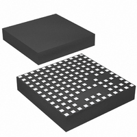
LTM4611EV#PBF Linear Technology, LTM4611EV#PBF Datasheet - Page 12

LTM4611EV#PBF
Manufacturer Part Number
LTM4611EV#PBF
Description
IC UMODULE DC/DC LV 15A 133-LGA
Manufacturer
Linear Technology
Series
µModuler
Type
Point of Load (POL) Non-Isolatedr
Datasheet
1.LTM4611EVPBF.pdf
(28 pages)
Specifications of LTM4611EV#PBF
Output
0.8 ~ 5 V
Number Of Outputs
1
Power (watts)
75W
Mounting Type
Surface Mount
Voltage - Input
1.5 ~ 5.5 V
Package / Case
133-LGA
1st Output
0.8 ~ 5 VDC @ 15A
Size / Dimension
0.59" L x 0.59" W x 0.17" H (15mm x 15mm x 4.32mm)
Power (watts) - Rated
75W
Operating Temperature
-40°C ~ 125°C
Efficiency
94%
Lead Free Status / RoHS Status
Lead free / RoHS Compliant
3rd Output
-
2nd Output
-
Available stocks
Company
Part Number
Manufacturer
Quantity
Price
LTM4611
applicaTions inForMaTion
For a buck converter, the switching duty cycle can be
estimated as:
Without considering the inductor current ripple, for each
output, the RMS current of the input capacitor can be
estimated as:
In the above equation, η% is the estimated efficiency of the
power module. The bulk capacitor can be a switcher-rated
electrolytic aluminum capacitor or a Polymer capacitor.
Output Capacitors
The LTM4611 is designed for low output voltage ripple
noise. The bulk output capacitors defined as C
chosen with low enough effective series resistance (ESR)
to meet the output voltage ripple and transient require-
ments. C
low ESR Polymer capacitor or ceramic capacitors. The
typical output capacitance range is from 200µF to 800µF.
Additional output filtering may be required by the system
designer, if further reduction of output ripple or dynamic
transient spikes is required. Table 5 shows a matrix of dif-
ferent output voltages and output capacitors to minimize
the voltage droop and overshoot during a 7A/µs transient.
The table optimizes total equivalent ESR and total bulk
capacitance to optimize the transient performance. Stabil-
ity criteria are considered in the Table 5 matrix, and the
Linear Technology µModule Power Design Tool will be
provided for stability analysis. Multiphase operation will
reduce effective output ripple as a function of the num-
ber of phases. Application Note 77 discusses this noise
reduction versus output ripple current cancellation, but
the output capacitance should be considered carefully as
a function of stability and transient response. The Linear
Technology µModule Power Design Tool can calculate the
output ripple reduction as the number of implemented
phase’s increases by N times.
D =
I
CIN(RMS)
V
V
OUT
OUT
IN
=
can be the low ESR tantalum capacitor, the
I
OUT(MAX)
η%
• D •(1– D)
OUT
are
Burst Mode Operation
The LTM4611 is capable of Burst Mode operation in which
the power MOSFETs operate intermittently based on load
demand, thus saving quiescent current. For applications
where maximizing the efficiency at very light loads is a high
priority, Burst Mode operation should be applied. To enable
Burst Mode operation, simply leave the MODE_PLLIN pin
floating. During Burst Mode operation, the peak current of
the inductor is set to approximately 33% of the maximum
peak current value in normal operation even though the
voltage at the I
at the I
greater than the load requirement. As the I
below 0.5V, the burst comparator trips, causing the internal
sleep line to go high and turn off both power MOSFETs.
In this sleep mode, the internal circuitry is partially turned
off, reducing the LTM4611’s quiescent current while the
load current is supplied by the output capacitors. When
the output voltage drops–causing I
sleep line goes low and the LTM4611 resumes normal
operation. The next oscillator cycle turns on the top power
MOSFET and the switching cycle repeats.
Pulse-Skipping Mode Operation
In applications where low output ripple and high effi-
ciency at intermediate currents are desired, pulse-skipping
mode should be used. Pulse-skipping operation allows
the LTM4611 to skip cycles at low output loads, thus
increasing efficiency by reducing switching loss. Tying
the MODE_PLLIN pin to INTV
operation. With pulse-skipping mode at light load, the
internal current comparator may remain tripped for several
cycles, thus skipping operation cycles. This mode has lower
ripple than Burst Mode operation and maintains a higher
frequency operation than Burst Mode operation.
Forced Continuous Operation
In applications where fixed frequency operation is more
critical than low current efficiency, and where the lowest
output ripple is desired, forced continuous operation
should be used. Forced continuous operation can be
TH
pin drops when the inductor’s average current is
TH
pin indicates a lower value. The voltage
CC
enables pulse-skipping
TH
to rise–the internal
TH
voltage drops
4611f


