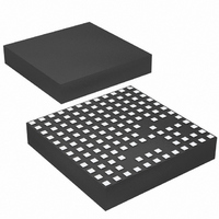
LTM4611EV#PBF Linear Technology, LTM4611EV#PBF Datasheet - Page 11

LTM4611EV#PBF
Manufacturer Part Number
LTM4611EV#PBF
Description
IC UMODULE DC/DC LV 15A 133-LGA
Manufacturer
Linear Technology
Series
µModuler
Type
Point of Load (POL) Non-Isolatedr
Datasheet
1.LTM4611EVPBF.pdf
(28 pages)
Specifications of LTM4611EV#PBF
Output
0.8 ~ 5 V
Number Of Outputs
1
Power (watts)
75W
Mounting Type
Surface Mount
Voltage - Input
1.5 ~ 5.5 V
Package / Case
133-LGA
1st Output
0.8 ~ 5 VDC @ 15A
Size / Dimension
0.59" L x 0.59" W x 0.17" H (15mm x 15mm x 4.32mm)
Power (watts) - Rated
75W
Operating Temperature
-40°C ~ 125°C
Efficiency
94%
Lead Free Status / RoHS Status
Lead free / RoHS Compliant
3rd Output
-
2nd Output
-
Available stocks
Company
Part Number
Manufacturer
Quantity
Price
applicaTions inForMaTion
The typical LTM4611 application circuit is shown in
Figure 21. External component selection is primarily
determined by the maximum load current and output
voltage. Refer to Table 5 for specific external capacitor
requirements for particular applications.
V
There are restrictions in the V
ratio that can be achieved for a given input voltage. The
V
current at very low input voltages. A dropout voltage of
300mV from input to output of LTM4611 is achievable
at 15A load, but reflected input voltage ripple and noise
should be taken into consideration in such applications.
Additionally, the transient-handling capability of the source
supply feeding LTM4611 can become an important factor
in truly achieving ultralow dropout at high output current.
For example, V
LTM4611 responds to heavy transient step loads on its
output, if insufficient input bypass capacitance is used in
combination with a sluggish source supply.
When V
when the caliber of the source supply is in question, it
is recommended to evaluate the amount and quality of
input bypass capacitance needed to maintain one’s target
dropout voltage with the source supply that will be used
in the end application. Demo Board DC1588A can be used
for such evaluation.
At very low duty cycles the minimum specified on-time
must be maintained. See the Frequency Adjustment sec-
tion and temperature derating curves.
To prevent overstress to the µpower bias generator, do
not ramp up V
is difficult to violate this guideline.) There is no restriction
on how rapidly V
Output Voltage Programming
The PWM controller has an internal 0.8V ±1.75% reference
voltage over temperature. As shown in the Block Diagram,
a 60.4k internal feedback resistor connects the V
and V
IN
IN
to V
to V
FB
OUT
OUT
OUT
pins together. When the remote sense amplifier
minimum dropout is still a function of its load
Step-Down Ratios
is expected to be within 600mV of V
IN
IN
at a rate exceeding 5V/µs (in practice, it
can sag or overshoot dramatically when
IN
may be discharged.
IN
to V
OUT
step-down
OUT_LCL
IN
, or
is used, then DIFFV
If the remote sense amplifier is not used, then V
connects to V
with no feedback resistor. Adding a resistor R
to GND programs the output voltage:
Table 1. V
V
R
For parallel operation of N LTM4611s, the following equa-
tion can be used to solve for R
Tie the V
COMP, TRACK/SS, V
tied together as shown in Figures 18 and 19.
For parallel applications, best noise immunity can be
achieved by placing capacitors of value C
and value C
If space limitations impede realizing this, then placement
of capacitors of value N • C
N • C
Input Capacitors
The LTM4611 module should be connected to a low
AC impedance DC source. Additional input capacitors
are needed for the RMS input ripple current rating. The
I
the input capacitor requirement. Typically 22µF X7R ce-
ramics are a good choice with RMS ripple current ratings
of ~2A each. A 100µF to 150µF surface mount aluminum
electrolytic bulk capacitor can be used for more input
bulk capacitance. This bulk input capacitor is only needed
if the input source impedance is compromised by long
inductive leads, traces or not enough source capacitance.
If low impedance power planes are used, then this bulk
capacitor is not needed.
CIN(RMS)
OUT
FB
R
V
(kΩ) Open
OUT
FB
FF
=
from V
= 0.8V •
FB
0.8V
60.4k / N
FB
equation which follows can be used to calculate
0.8V
V
OUT
Resistor Table vs Various Output Voltages
FF
pins together for each parallel output. The
OUT
from V
OUT
1.0V
– 1
243
60.4k +R
. The output voltage will default to 0.8V
to the bussed V
OUT
OUT_LCL
R
OUT
1.2V
121
FB
is connected to the V
to V
FB
P
1.5V
68.1
, and RUN pins must also be
from V
FB
FB
, local to each µModule.
:
1.8V
47.5
FB
FB
signal, can suffice.
to GND, and value
LTM4611
P
2.5V
28.0
from V
OUT_LCL
FB
3.3V
19.1
FB
from V
OUT_LCL
to GND,
5.0V
11.5
pin.
4611f
FB


