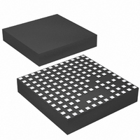
LTM4611EV#PBF Linear Technology, LTM4611EV#PBF Datasheet - Page 23

LTM4611EV#PBF
Manufacturer Part Number
LTM4611EV#PBF
Description
IC UMODULE DC/DC LV 15A 133-LGA
Manufacturer
Linear Technology
Series
µModuler
Type
Point of Load (POL) Non-Isolatedr
Datasheet
1.LTM4611EVPBF.pdf
(28 pages)
Specifications of LTM4611EV#PBF
Output
0.8 ~ 5 V
Number Of Outputs
1
Power (watts)
75W
Mounting Type
Surface Mount
Voltage - Input
1.5 ~ 5.5 V
Package / Case
133-LGA
1st Output
0.8 ~ 5 VDC @ 15A
Size / Dimension
0.59" L x 0.59" W x 0.17" H (15mm x 15mm x 4.32mm)
Power (watts) - Rated
75W
Operating Temperature
-40°C ~ 125°C
Efficiency
94%
Lead Free Status / RoHS Status
Lead free / RoHS Compliant
3rd Output
-
2nd Output
-
Available stocks
Company
Part Number
Manufacturer
Quantity
Price
applicaTions inForMaTion
Safety Considerations
The LTM4611 modules do not provide galvanic isolation
from V
a slow blow fuse with a rating twice the maximum input
current needs to be provided to protect each unit from
catastrophic failure. The device does support overvoltage
protection and overcurrent protection.
Layout Checklist/Example
The high integration of LTM4611 makes the PCB board
layout very simple and easy. However, to optimize its
electrical and thermal performance, some layout consid-
erations are still necessary.
• Use large PCB copper areas for high current paths,
• Place high frequency ceramic input and output capaci-
• Place a dedicated power ground layer underneath the
including V
PCB conduction loss and thermal stress.
tors next to the V
high frequency noise.
unit.
IN
to V
OUT
IN
, GND and V
. There is no internal fuse. If required,
IN
, GND and V
V
V
GND
OUT
IN
OUT
C
OUT
. It helps to minimize the
C
IN
OUT
C
OUT
pins to minimize
C
Figure 17. Recommended PCB Layouts
IN
• To minimize the via conduction loss and reduce module
• Do not put vias directly on the pad, unless they are
• Use a separated SGND ground copper area for com-
• For parallel modules, tie the respective COMP, V
• To facilitate stuffing verification, test and debug activi-
thermal stress, use multiple vias for interconnection
between top layer and other power layers.
capped or plated over.
ponents connected to signal pins. Connect the SGND
to GND underneath the unit.
V
internal layer to closely connect these pins together.
Figure 17 gives a good example of the recommended
layout. Figures 18 and 19 show schematics of the
LTM4611 devices operating in parallel.
ties, consider routing control signals of the LTM4611
with short traces to localized test points, test pads or
test vias–as PCB layout space permits. Both in-house
and contract manufacturers enjoy gaining electrical
access to all non low impedance (>10Ω) pins of an
IC or µModule device to improve in-circuit test (ICT)
coverage.
OUT_LCL
, TRACK/SS and RUN pins together. Use an
CONTROL
V
OUT
4611 F17
SIGNAL
GROUND
LTM4611
4611f
FB
,


