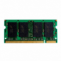
MT16LSDF6464HG-133D2 Micron Technology Inc, MT16LSDF6464HG-133D2 Datasheet

MT16LSDF6464HG-133D2
Specifications of MT16LSDF6464HG-133D2
Available stocks
Related parts for MT16LSDF6464HG-133D2
MT16LSDF6464HG-133D2 Summary of contents
Page 1
... PRODUCTS AND SPECIFICATIONS DISCUSSED HEREIN ARE FOR EVALUATION AND REFERENCE PURPOSES ONLY AND ARE SUBJECT TO CHANGE BY MICRON WITHOUT NOTICE. PRODUCTS ARE ONLY WARRANTED BY MICRON TO MEET MICRON’S PRODUCTION DATA SHEET SPECIFICATIONS. MT16LSDF3264HG, MT16LSDF6464HG For the latest data sheet, please refer to the Micron Web site: www ...
Page 2
... GENERAL DESCRIPTION ® The Micron MT16LSDF3264HG MT16LSDF6464HG are high-speed CMOS, dynamic random-access, 256MB and 512MB memory modules, organized in a x64 configuration. These modules use SDRAMs that are internally configured as quad-bank DRAMs with a synchronous interface (all signals are registered on the positive edge of the clock signal CK0). ...
Page 3
... A0-A12: SDRAMs U1-U16 BA0, BA1: SDRAMs U1-U16 CS# (U1-U8) CS# (U9-U16) CKE (U1-U8) CKE (U9-U16) SDRAMs U1-U17 SDRAMs U1-U17 MT16LSDF3264HG (256MB): MT16LSDF6464HG (512MB): Micron Technology, Inc., reserves the right to change products or specifications without notice. 3 PRELIMINARY 256/512MB (x64) SDRAM SODIMM 22 Ω S1# DQMB4 S0# DQM CS# CS# DQM ...
Page 4
PIN DESCRIPTIONS SYMBOL RAS#, CAS#, WE# CK0, CK1 CKE0, CKE1 S0#, S1# DQMB0–DQMB7 BA0, BA1 A0-A12 SCL DQ0–DQ63 SDA 32/64 Meg x 64 SDRAM SODIMM SD16C32_64x64HG_A.pm6; Rev. A, Pub 7/01 TYPE Input Command Inputs RAS#, CAS#, ...
Page 5
... Reserved for Future Use – Do Not Use: This pin is not connected on these modules but is an assigned pin on the compatible DRAM version. – No Connect: These pins should be left unconnected. Micron Technology, Inc., reserves the right to change products or specifications without notice. ...
Page 6
... SDRAM COMPONENT DESCRIPTION In general, the 128MB and 256Mb SDRAM memory devices used for these modules are quad-bank DRAMs, that operate at 3.3V and include a synchro- nous interface (all signals are registered on the positive edge of the clock signal, CLK). The four banks of a x8, 128Mb device are each configured as 4,096 bit-rows, by 512 bit-columns input/output bits ...
Page 7
CAS Latency The CAS latency is the delay, in clock cycles, be- tween the registration of a READ command and the availability of the first piece of output data. The la- tency can be set to two or three clocks. ...
Page 8
Burst Type Accesses within a given burst may be programmed to be either sequential or interleaved; this is referred to as the burst type and is selected via bit M3. The ordering of accesses within a burst is deter- mined ...
Page 9
COMMANDS The following Truth Table provides a general refer- ence of available commands. For a more detailed descrip- TRUTH TABLE – SDRAM COMMANDS AND DQMB OPERATION (Note: 1) NAME (FUNCTION) COMMAND INHIBIT (NOP) NO OPERATION (NOP) ACTIVE (Select bank and ...
Page 10
ABSOLUTE MAXIMUM RATINGS* Voltage Supply DD DD Relative to V ....................................... -1V to +4.6V SS Voltage on Inputs I/O Pins Relative to V ....................................... -1V to +4.6V SS Operating Temperature, T (commercial) ....................................... ...
Page 11
... AUTO REFRESH CURRENT CS# = HIGH; CKE = HIGH SELF REFRESH CURRENT: CKE ≤ 0.2V I SPECIFICATIONS AND CONDITIONS (Notes 11, 13; notes appear following the parameter tables) (V PARAMETER/CONDITION - MT16LSDF6464HG OPERATING CURRENT: Active Mode; t Burst = 2; READ or WRITE STANDBY CURRENT: Power-Down Mode; All banks idle; CKE = LOW STANDBY CURRENT: Active Mode ...
Page 12
CAPACITANCE (Note 2; notes appear following parameter tables) PARAMETER Input Capacitance: A0-A12, BA0, BA1, RAS#, CAS#, WE# Input Capacitance: CK0-CK3 Input Capacitance: S0#-S3# Input Capacitance: CKE0, CKE1 Input Capacitance: DQMB0-DQMB7 Input/Output Capacitance: SCL, SA0-SA2, SDA Input/Output Capacitance: DQ0-DQ63 ELECTRICAL CHARACTERISTICS ...
Page 13
AC FUNCTIONAL CHARACTERISTICS (Notes 11, 31; notes appear following the parameter tables) (0°C ≤ T PARAMETER READ/WRITE command to READ/WRITE command CKE to clock disable or power-down entry mode CKE to clock enable or power-down ...
Page 14
NOTES 1. All voltages referenced This parameter is sampled MHz 25°C; pin under test biased at 1.4V dependent on output loading and cycle rates. DD Specified ...
Page 15
SPD CLOCK AND DATA CONVENTIONS Data states on the SDA line can change only during SCL LOW. SDA state changes during SCL HIGH are reserved for indicating start and stop conditions as indicated in Figures 3 and 4. SPD START ...
Page 16
EEPROM DEVICE SELECT CODE The most significant bit (b7) is sent first Memory Area Select Code (two arrays) Protection Register Select Code EEPROM OPERATING MODES MODE RW BIT Current Address Read 1 Random Address Read 0 1 Sequential Read 1 ...
Page 17
SERIAL PRESENCE-DETECT EEPROM DC OPERATING CONDITIONS (Note +3.3V ±0.3V) DD PARAMETER/CONDITION SUPPLY VOLTAGE INPUT HIGH VOLTAGE: Logic 1; All inputs INPUT LOW VOLTAGE: Logic 0; All inputs OUTPUT LOW VOLTAGE 3mA OUT INPUT LEAKAGE CURRENT: ...
Page 18
... RCD 15 (-13E) 20 (-133/-10E) 45 (-13E)* 44 (-133) 50 (-10E RP. Actual device spec value is 37ns. Micron Technology, Inc., reserves the right to change products or specifications without notice. 18 PRELIMINARY 256/512MB (x64) SDRAM SODIMM MT16LSDF6464HG ENTRY (VERSION) 80 128 08 256 04 SDRAM LVTTL 70 ...
Page 19
... MICRON 100/133 MHz Micron Technology, Inc., reserves the right to change products or specifications without notice. 19 PRELIMINARY 256/512MB (x64) SDRAM SODIMM MT16LSDF6464HG ENTRY (VERSION) 20 256MB 15 1.5 (-13E/-133 (-10E) 08 0.8 (--13E/133 (-10E) 15 1.5 (-13E/-133 (-10E) 08 0.8 (-13E/-133 (-10E) 00 ...
Page 20
R (2X) .071 (1.80) (2X) .236 (6.00) .100 (2.55) .079 (2.00) PIN 1 .83.82 (3.30) PIN 144 NOTE: All dimensions in inches (millimeters) MAX or typical where noted. DATA SHEET DESIGNATION Preliminary: This data sheet contains initial characterization ...


