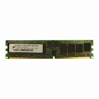
MT9VDDF6472Y-335F1 Micron Technology Inc, MT9VDDF6472Y-335F1 Datasheet - Page 21

MT9VDDF6472Y-335F1
Manufacturer Part Number
MT9VDDF6472Y-335F1
Description
MODULE DDR SDRAM 512MB 184-DIMM
Manufacturer
Micron Technology Inc
Specifications of MT9VDDF6472Y-335F1
Memory Type
DDR SDRAM
Memory Size
512MB
Speed
167MHz
Package / Case
184-DIMM
Main Category
DRAM Module
Sub-category
DDR SDRAM
Module Type
184RDIMM
Device Core Size
72b
Organization
64Mx72
Total Density
512MByte
Chip Density
512Mb
Maximum Clock Rate
333MHz
Operating Supply Voltage (typ)
2.5V
Operating Current
1.575A
Number Of Elements
9
Operating Supply Voltage (max)
2.7V
Operating Supply Voltage (min)
2.3V
Operating Temp Range
0C to 70C
Operating Temperature Classification
Commercial
Pin Count
184
Mounting
Socket
Lead Free Status / RoHS Status
Lead free / RoHS Compliant
Other names
557-1293
MT9VDDF6472Y-335F1
MT9VDDF6472Y-335F1
pdf: 09005aef80e119b2, source: 09005aef807d56a1
DDF9C32_64x72G.fm - Rev. B 9/04 EN
22. The valid data window is derived by achieving
23. Each byte lane as a corresponding DQS.
25. To maintain a valid level, the transitioning edge of
24. This limit is actually a nominal value and does not
by the DRAM controller greater than eight refresh
cycles is not allowed.
other specifications:
(
directly porportional with the clock duty cycle
and a practical data valid window can be derived.
The clock is allowed a maximum duty cycle varia-
tion of 45/55. Functionality is uncertain when
operating beyond a 45/55 ratio. Figure 9, Derating
Data Valid Window, shows derating curves for
duty cycles between 50/50 and 45/55.
result in a fail value. CKE is HIGH during REFRESH
command period (
during standby).
the input must:
3.8
3.6
3.4
3.2
3.0
2.8
2.6
2.4
2.2
2.0
1.8
a. Sustain a constant slew rate from the current
t
QH =
AC level through to the target AC level, V
or V
50/50
t
IH
3.750
HP -
2.500
3.400
(AC).
t
NA
QHS). The data valid window derates
49.5/50.5
3.700
-335
-262/-26A/-265 @ t CK = 10ns
-202 @ t CK = 10ns
-262/-26A/-265 @ t CK = 7.5ns
t
RFC [MIN]) else CKE is LOW (i.e.,
3.350
2.463
t
HP (
t
3.650
49/51
Figure 9: Derating Data Valid Window
CK/2),
2.425
3.300
t
48.5/52.5
DQSQ, and
3.600
2.388
3.250
IL
3.550
48/52
(AC)
t
(
QH
t
2.350
3.200
QH –
Clock Duty Cycle
21
t
DQSQ)
47.5/53.5
3.500
26. JEDEC specifies CK and CK# input slew rate must
27. DQ and DM input slew rates must not deviate
28. V
29. The clock is allowed up to ±150ps of jitter. Each
30.
2.313
3.150
be 1V/ns (2V/ns differentially).
from DQS by more than 10 percent. If the DQ/
DM/DQS slew rate is less than 0.5V/ns, timing
must be derated: 50ps must be added to
t
slew rate exceeds 4V/ns, functionality is uncertain.
For -335, slew rates must be 0.5 V/ns.
not active while any bank is active.
timing parameter is allowed to vary by the same
amount.
t
minimum actually applied to the device CK and
CK# inputs, collectively during bank active.
b. Reach at least the target AC level.
c. After the AC target level is reached, continue to
DH for each 100mv/ns reduction in slew rate. If
HP min is the lesser of
256MB, 512MB (x72, ECC, SR)
Micron Technology, Inc., reserves the right to change products or specifications without notice.
DD
184-PIN DDR SDRAM RDIMM
maintain at least the target DC level, V
or V
47/53
3.450
must not vary more than 4 percent if CKE is
2.275
3.100
IH
(DC).
46.5/54.5
3.400
2.238
3.050
3.350
46/54
©2004 Micron Technology, Inc. All rights reserved.
2.200
3.000
t
CL minimum and
45.5/55.5
3.300
2.163
2.950
t
3.250
45/55
DS and
IL
2.125
2.900
(DC)
t
CH


