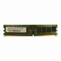
MT9VDDF6472Y-335F1 Micron Technology Inc, MT9VDDF6472Y-335F1 Datasheet - Page 16

MT9VDDF6472Y-335F1
Manufacturer Part Number
MT9VDDF6472Y-335F1
Description
MODULE DDR SDRAM 512MB 184-DIMM
Manufacturer
Micron Technology Inc
Specifications of MT9VDDF6472Y-335F1
Memory Type
DDR SDRAM
Memory Size
512MB
Speed
167MHz
Package / Case
184-DIMM
Main Category
DRAM Module
Sub-category
DDR SDRAM
Module Type
184RDIMM
Device Core Size
72b
Organization
64Mx72
Total Density
512MByte
Chip Density
512Mb
Maximum Clock Rate
333MHz
Operating Supply Voltage (typ)
2.5V
Operating Current
1.575A
Number Of Elements
9
Operating Supply Voltage (max)
2.7V
Operating Supply Voltage (min)
2.3V
Operating Temp Range
0C to 70C
Operating Temperature Classification
Commercial
Pin Count
184
Mounting
Socket
Lead Free Status / RoHS Status
Lead free / RoHS Compliant
Other names
557-1293
MT9VDDF6472Y-335F1
MT9VDDF6472Y-335F1
Table 13: IDD Specifications and Conditions – 512MB
DDR SDRAM components only
Notes: 1–5, 8, 10, 12, 48; notes appear on pages 20–23; 0°C
pdf: 09005aef80e119b2, source: 09005aef807d56a1
DDF9C32_64x72G.fm - Rev. B 9/04 EN
PARAMETER/CONDITION
OPERATING CURRENT: One device bank; Active-Precharge;
t
changing once per clock cyle; Address and control inputs
changing once every two clock cycles
OPERATING CURRENT: One device bank; Active -Read Precharge;
Burst = 4;
I
cycle
PRECHARGE POWER-DOWN STANDBY CURRENT: All device banks
idle; Power-down mode;
IDLE STANDBY CURRENT: CS# = HIGH; All device banks idle;
t
once per clock cycle. V
ACTIVE POWER-DOWN STANDBY CURRENT: One device bank
active; Power-down mode;
CKE = LOW
ACTIVE STANDBY CURRENT: CS# = HIGH; CKE = HIGH; One device
bank; Active-Precharge;
t
clock cycle; Address and other control inputs changing once per
clock cycle
OPERATING CURRENT: Burst = 2; Reads; Continuous burst; One
bank active; Address and control inputs changing once per clock
cycle;
OPERATING CURRENT: Burst = 2; Writes; Continuous burst; One
device bank active; Address and control inputs changing once
per clock cycle;
changing twice per clock cycle
AUTO REFRESH CURRENT
SELF REFRESH CURRENT: CKE
OPERATING CURRENT: Four device bank interleaving READs (BL =
4) with auto precharge,
t
Active READ, or WRITE commands
OUT
RC =
CK MIN; CKE = HIGH; Address and other control inputs changing
CK =
CK =
= 0mA; Address and control inputs changing once per clock
t
t
t
t
RC (MIN);
CK (MIN); DQ, DM andDQS inputs changing twice per
CK (MIN); Address and control inputs change only during
CK =
t
RC =
t
CK (MIN); I
t
t
CK =
t
RC (MIN);
CK =
t
CK (MIN); DQ, DM, and DQS inputs
t
IN
CK (MIN); DQ, DM and DQS inputs
OUT
t
t
= V
RC =
RC =
t
CK =
t
CK =
t
= 0mA
REF
CK =
t
t
RC (MIN);
RAS (MAX);
t
0.2V
for DQ, DQS, and DM
CK (MIN); CKE = (LOW)
t
CK (MIN);
t
CK (MIN);
t
t
REFC =
REFC = 7.8125µs
t
RFC (MIN)
t
CK =
16
T
A
+70°C; V
I
I
I
SYM
I
I
I
I
DD4W
I
I
DD3N
I
DD5A
I
I
DD2P
DD3P
DD4R
DD2F
DD 0
DD1
DD5
DD6
DD7
256MB, 512MB (x72, ECC, SR)
Micron Technology, Inc., reserves the right to change products or specifications without notice.
184-PIN DDR SDRAM RDIMM
DD
= V
1,170
1,440
1,485
1,575
2,610
3,645
-335
405
315
450
45
90
45
DD
Q = +2.5V ±0.2V
MAX
1,170
1,440
1,485
1,395
2,610
3,600
-262
405
315
450
45
90
45
©2004 Micron Technology, Inc. All rights reserved.
-26A/
-265/
1,035
1,305
1,305
1,215
2,520
3,150
-202
360
270
405
45
90
45
UNITS
mA
mA
mA
mA
mA
mA
mA
mA
mA
mA
mA
mA
NOTES
21, 28,
21, 28,
20, 42
20, 42
20, 42
20, 44
24, 44
20, 43
44
45
44
41
20
9


