MT9VDDF6472Y-335F1 Micron Technology Inc, MT9VDDF6472Y-335F1 Datasheet
MT9VDDF6472Y-335F1
Specifications of MT9VDDF6472Y-335F1
MT9VDDF6472Y-335F1


Related parts for MT9VDDF6472Y-335F1


MT9VDDF6472Y-335F1 Summary of contents
Page 1
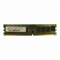
... ECC, SR) 184-PIN DDR SDRAM RDIMM MT9VDDF3272 – 256MB MT9VDDF6472 – 512MB For the latest data sheet, please refer to the Micron site: www.micron.com/products/modules Figure 1: 184-Pin DIMM (MO-206) Low-Profile 1.125in. (28.58mm) 256MB Low-Profile 1.125in. (28.58mm) 512MB Very Low-Profile 0.72in. (18.29mm) OPTIONS • ...
Page 2
... MT9VDDF6472G-335__ MT9VDDF6472Y-335__ 512MB MT9VDDF6472G-262__ 512MB MT9VDDF6472Y-262__ 512MB 512MB MT9VDDF6472G-26A__ 512MB MT9VDDF6472Y-26A__ MT9VDDF6472(I)G-265__ 512MB MT9VDDF6472(I)Y-265__ 512MB 512MB MT9VDDF6472(I)G-202__ 512MB MT9VDDF6472(I)Y-202__ NOTE: All part numbers end with a two-place code (not shown), designating component and PCB revisions. Consult factory for current revision codes. Example: MT9VDDF3272G-265B1. ...
Page 3
Table 3: Pin Assignment (184-Pin DIMM Front) PIN SYMBOL PIN SYMBOL PIN SYMBOL PIN SYMBOL DQ17 47 REF 2 DQ0 25 DQS2 DQ1 DQS0 ...
Page 4
Table 5: Pin Descriptions Pin numbers may not correlate with symbols. Refer to Pin Assignment tables on page 3 for more information PIN NUMBERS SYMBOL 10 63, 65, 154 WE#, CAS#, RAS# 137, 138 CK0, CK0# 21 157 52, 59 ...
Page 5
... Supply Ground. SS Supply Serial EEPROM positive power supply: . DDSPD DNU — Do Not Use: Thes pins are not connected on these modules, but are assigned pins on other modules in this product family NC — No Connect: These pins should be left unconnected. 5 256MB, 512MB (x72, ECC, SR) ...
Page 6
... RRAS#: DDR SDRAMs S RCAS#: DDR SDRAMs T RCKE0: DDR SDRAMs E RWE#: DDR SDRAMs R S RESET# Standard modules use the following DDR SDRAM devices: Lead-free modules use the following DDR SDRAM devices: www.micron.com/num- 6 256MB, 512MB (x72, ECC, SR) 184-PIN DDR SDRAM RDIMM DM CS# DQS DQ DQ32 DQ DQ33 DQ ...
Page 7
... RRAS#: DDR SDRAMs S RCAS#: DDR SDRAMs T RCKE0: DDR SDRAMs E RWE#: DDR SDRAMs R S RESET# Standard modules use the following DDR SDRAM devices: Lead-free modules use the following DDR SDRAM devices: www.micron.com/num- 7 256MB, 512MB (x72, ECC, SR) 184-PIN DDR SDRAM RDIMM DM CS# DQS DQ DQ32 DQ DQ33 DQ ...
Page 8
... RCKE0: DDR SDRAMs RWE#: DDR SDRAMs RESET Standard modules use the following DDR SDRAM devices: MT46V32M8FG (256MB); MT46V64M8FG (512MB) Lead-free modules use the following DDR SDRAM devices: www.micron.com/num- MT46V32M8BG (256MB); MT46V64M8BG (512MB) Micron Technology, Inc., reserves the right to change products or specifications without notice. 8 ...
Page 9
... DDR SDRAM modules use internally con- figured quad-bank DDR SDRAM devices. DDR SDRAM modules use a double data rate archi- tecture to achieve high-speed operation. The double data rate architecture is essentially a 2n-prefetch architecture with an interface designed to transfer two data words per clock cycle at the I/O pins ...
Page 10
Vio- lating either of these requirements will result in unspecified operation. Mode register bits A0–A2 specify the burst length, A3 specifies the type of burst (sequential ...
Page 11
Table 6: Burst Definition Table ORDER OF ACCESSES WITHIN STARTING BURST COLUMN TYPE = LENGTH ADDRESS SEQUENTIAL 0 0-1-2 1-2-3 2-3-0 3-0-1 ...
Page 12
DLL should always be followed by a LOAD MODE REGISTER command to the mode regis- ter (BA0/BA1 both LOW) to ...
Page 13
Commands Table 8, Commands Truth Table, and Table 9, DM Operation Truth Table, provide a general reference of available commands. For a more detailed description Table 8: Commands Truth Table CKE is HIGH for all commands shown except SELF REFRESH; ...
Page 14
Absolute Maximum Ratings Stresses greater than those listed under “Absolute Maximum Ratings” may cause permanent damage to the device. This is a stress rating only, and functional operation of the device at these or any other condi- Voltage on V ...
Page 15
Table 12: IDD Specifications and Conditions – 256MB DDR SDRAM components only Notes: 1–5, 8, 10, 12, 48; notes appear on pages 20–23; 0°C PARAMETER/CONDITION OPERATING CURRENT: One device bank; Active-Precharge (MIN (MIN); ...
Page 16
Table 13: IDD Specifications and Conditions – 512MB DDR SDRAM components only Notes: 1–5, 8, 10, 12, 48; notes appear on pages 20–23; 0°C PARAMETER/CONDITION OPERATING CURRENT: One device bank; Active-Precharge (MIN); CK ...
Page 17
Table 14: Capacitance Note: 11; notes appear on pages 20–23 PARAMETER Input/Output Capacitance: DQ, DQS, DM Input Capacitance: Command and Address, S#, CKE Input Capacitance: CK, CK# Table 15: DDR SDRAM Component Electrical Characteristics and Recommended AC Operating Conditions (-335, ...
Page 18
Table 15: DDR SDRAM Component Electrical Characteristics and Recommended AC Operating Conditions (-335, -262) (Continued) Notes: 1–5, 8, 10, 12; notes appear on pages 20–23; 0°C AC CHARACTERISTICS PARAMETER DQS read preamble DQS read postamble ACTIVE bank a to ACTIVE ...
Page 19
Table 16: DDR SDRAM Component Electrical Characteristics and Recommended AC Operating Conditions (-26A, -265, -202) (Continued) Notes: 1–5, 8, 10, 12; notes appear on pages 20–23; 0°C AC CHARACTERISTICS PARAMETER Address and control input hold time (slow slew rate) Address ...
Page 20
Notes 1. All voltages referenced Tests for AC timing and electrical AC and DC DD characteristics may be conducted at nominal ref- erence/supply voltage levels, but the related spec- ifications and device operation are ...
Page 21
DRAM controller greater than eight refresh cycles is not allowed. 22. The valid data window is derived by achieving t t other specifications CK/2 QHS). The data valid ...
Page 22
READs and WRITEs with auto precharge are not t allowed to be issued until RAS(MIN) can be satis- fied prior to the internal precharge command being issued. 32. Any positive glitch in the nominal voltage must be less than ...
Page 23
Random addressing changing and 50 percent of data changing at every transfer. 43. Random addressing changing and 100 percent of data changing at every transfer. 44. CKE must be active (high) during the entire time a refresh command is ...
Page 24
Initialization To ensure device operation the DRAM must be ini- tialized as described below: 1. Simultaneously apply power Apply V and then V power. REF TT 3. Assert and hold CKE at a LVCMOS logic low. 4. ...
Page 25
Table 17: Register Timing Requirements and Switching Characteristics Note: 1 REGISTER SYMBOL PARAMERTER f Clock Frequency clock t Clock to Output Time pd t Reset to Output Time PHL SSTL t Pulse Duration w (bit pattern by JESD82-3 t Differential ...
Page 26
Table 18: PLL Clock Driver Timing Requirements and Switching Characteristics Note: 1 PARAMETER SYMBOL Operating Clock Frequency Input Duty Cycle Stabilization Time Cycle to Cycle Jitter Static Phase Offset Output Clock Skew Period Jitter Half-Period Jitter t Input Clock Slew ...
Page 27
SPD Clock and Data Conventions Data states on the SDA line can change only during SCL LOW. SDA state changes during SCL HIGH are reserved for indicating start and stop conditions (Fig- ure 13, Data Validity, and Figure 14, Definition ...
Page 28
Table 19: EEPROM Device Select Code The most significant bit (b7) is sent first SELECT CODE Memory Area Select Code (two arrays) Protection Register Select Code Table 20: EEPROM Operating Modes MODE Current Address Read Random Address Read Sequential Read ...
Page 29
Table 21: Serial Presence-Detect EEPROM DC Operating Conditions All voltages referenced DDSPD PARAMETER/CONDITION Supply Voltage Input High Voltage: Logic 1; All inputs Input Low Voltage: Logic 0; All inputs Output Low Voltage 3mA ...
Page 30
Table 23: Serial Presence-Detect Matrix “1”/“0”: Serial Data, “driven to HIGH”/“driven to LOW” BYTE DESCRIPTION 0 Number of SPD Bytes Used by Micron 1 Total Number of Bytes in SPD Device 2 Fundamental Memory Type 3 Number of Row Addresses ...
Page 31
Table 23: Serial Presence-Detect Matrix “1”/“0”: Serial Data, “driven to HIGH”/“driven to LOW” BYTE DESCRIPTION 31 Module Rank Density 32 Address and Command Setup Time, note 3) 33 Address and Command Hold Time, note 3) 34 Data/ Data Mask Input ...
Page 32
... The value of RAS used for -26A/-265 modules is calculated from 3. The JEDEC SPD specification allows fast or slow slew rate values for these bytes. The worst-case (slow slew rate) value is repesented here. Systems requiring the fast slew rate setup and hold values are supported, provided the faster mini- mum slew rate is met ...
Page 33
Figure 17: 184-PIN DIMM Dimensions – Low-Profile 256MB 0.079 (2.00) R (4X 0.098 (2.50) D (2X) 0.091 (2.30) TYP. PIN 1 0.050 (1.27) TYP. 0.091 (2.30) 2.55 (64.77) TYP. No Components This Side of Module PIN 184 ...
Page 34
Figure 19: 184-PIN DIMM Dimensions – Very Low-Profile .00) R (4X 2.50) D (2X) 30) TYP. PIN 1 0.050 (1.27) TYP. 0.091 (2.30) 2.55 (64.77) TYP. PIN 184 Data Sheet Designation Released (No Mark): This data sheet ...