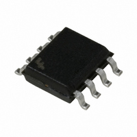
FAN6520AMX Fairchild Semiconductor, FAN6520AMX Datasheet - Page 10

FAN6520AMX
Manufacturer Part Number
FAN6520AMX
Description
IC CTRLR PWM SYNC BUCK SGL 8SOIC
Manufacturer
Fairchild Semiconductor
Type
Step-Down (Buck)r
Datasheet
1.FAN6520AMX.pdf
(15 pages)
Specifications of FAN6520AMX
Internal Switch(s)
No
Synchronous Rectifier
Yes
Number Of Outputs
1
Voltage - Output
0.8 ~ 5.5 V
Frequency - Switching
300kHz
Voltage - Input
4.5 ~ 5.5 V
Operating Temperature
0°C ~ 70°C
Mounting Type
Surface Mount
Package / Case
8-SOIC (3.9mm Width)
Power - Output
715mW
Topology
Boost, Buck
Output Voltage
0.8 V to 5.5 V
Switching Frequency
340 KHz
Duty Cycle (max)
100 %
Operating Supply Voltage
5 V
Maximum Operating Temperature
+ 70 C
Minimum Operating Temperature
0 C
Mounting Style
SMD/SMT
Synchronous Pin
No
Lead Free Status / RoHS Status
Lead free / RoHS Compliant
Current - Output
-
Lead Free Status / Rohs Status
Lead free / RoHS Compliant
Other names
FAN6520AMXTR
FAN6520AMX_NL
FAN6520AMX_NLTR
FAN6520AMX_NLTR
FAN6520AMX_NL
FAN6520AMX_NLTR
FAN6520AMX_NLTR
Available stocks
Company
Part Number
Manufacturer
Quantity
Price
Part Number:
FAN6520AMX_
Manufacturer:
FAIRCHILD/仙童
Quantity:
20 000
©2005 Fairchild Semiconductor Corporation
FAN6520A Rev. 1.0.5
1.25 times greater than the maximum input voltage. A
voltage rating of 1.5 times is a conservative guideline.
The RMS current rating requirement (I
capacitor of a buck regulator is:
where the converter duty cycle is
For a through-hole design, several electrolytic capacitors
may be needed. For surface-mount designs, solid tanta-
lum capacitors can be used, but caution must be exer-
cised with regard to the capacitor’s surge current rating.
The capacitors must be capable of handling the surge
current at power-up. Some capacitor series available
from reputable manufacturers are surge current tested.
Bootstrap Circuit
The bootstrap circuit uses a charge storage capacitor
(C
Select these components after the high-side MOSFET
has been chosen. The required capacitance is deter-
mined using the following equation:
where Q
FET and ΔV
high-side MOSFET drive. To prevent loss of gate drive,
the bootstrap capacitance should be at least 50 times
greater than the C
Thermal Considerations
Total device dissipation:
P
where P
P
where F
P
FET driver.
P
where P
rising and falling edges respectively.
where:
P
where Q
C BOOT
P
P
D
Q
HDRV
HDRV
Q1
H R
H F ( )
BOOT
= P
( )
= V
I
RMS
= Q
Q
CC
=
represents internal power dissipation of the upper
= P
=
) and the internal diode, as shown in Figure 1.
Q
SW
H(R)
G1
G1
G
+ P
P
=
P
=
represents quiescent power dissipation.
× [4mA + 0.036 (F
is the total gate charge of the high-side MOS-
H(R)
Q1
Q1
× V
is total gate charge of Q1 for its applied V
is switching frequency (in kHz).
I
HDRV
------------------------- -
ΔV BOOT
and P
L
BOOT
×
×
GS(Q1)
× P
(
Q G
------------------------------------------- -
R
------------------------------------------- -
R
D D
HDN
HUP
+ P
ISS
H(F)
H(F)
–
is the voltage droop allowed on the
R
× F
LDRV
R
of Q1.
2
+
+
are internal dissipations for the
)
HDN
HUP
R
R
SW
E
E
+
+
SW
R
R
G
G
– 100)]
D
=
RMS
V
--------------
V
OUT
IN
) for the input
.
(12)
(13)
(14)
(15)
(16)
(17)
(18)
(19)
GS
.
As described in the equations above, the total power
consumed in driving the gate is divided in proportion to
the resistances in series with the MOSFET's internal
gate node, as shown in Figure 9.
R
R
many designs. Note that the introduction of R
reduce driver power dissipation, but excess R
cause errors in the “adaptive gate drive” circuitry. For
more information, please refer to Application Note AN-
6003, “Shoot-through” in Synchronous Buck Converters
at
P
P
where P
rising and falling edges, respectively:
where:
P
Power MOSFET Selection
For more information on MOSFET selection for synchro-
nous buck regulators, refer to: AN-6005: Synchronous
Buck MOSFET Loss Calculations at
semi.com/an/AN/AN-6005.pdf.
Losses in a MOSFET are the sum of its switching (P
and conduction (P
In typical applications, the FAN6520A converter's output
voltage is low with respect to its input voltage; therefore
the lower MOSFET (Q2) is conducting the full load cur-
rent for most of the cycle. Choose a MOSFET for Q2 that
has low R
In contrast, the high-side MOSFET (Q1) has a much
shorter duty cycle and its conduction loss has less
impact. Q1, however, sees most of the switching losses,
so Q1’s primary selection criteria should be gate charge.
P
P
LDRV
LDRV
Q2
G
E
L R
L F ( )
10
http://www.fairchildsemi.com/an/AN/AN-6006.pdf.
( )
is the polysilicon gate resistance internal to the FET.
is the external gate drive resistor implemented in
= Q
=
is dissipation of the lower FET driver.
= P
=
BOOT
G2
H(R)
P
P
DS(ON)
Figure 9. Driver Dissipation Model
L(R)
Q2
Q2
× V
R
R
and P
HUP
HDN
×
×
× P
GS(Q2)
HDRV
------------------------------------------ -
R
------------------------------------------- -
R
to minimize conduction losses.
SW
HDN
LUP
L(F)
COND
H(F)
R
R
× F
+
+
LUP
LDN
) losses.
R
R
are internal dissipations for the
SW.
E
E
+
+
R
R
E
R
G
G
G
http://www.fairchild-
R
G
Q1
www.fairchildsemi.com
S
E
E
may
(20)
(23)
(21)
(22)
can
SW
)


