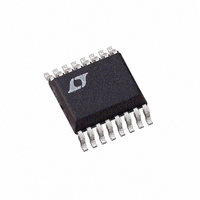
LTC3830EGN Linear Technology, LTC3830EGN Datasheet - Page 9

LTC3830EGN
Manufacturer Part Number
LTC3830EGN
Description
IC DC/DC CONTRLR STEP-DWN 16SSOP
Manufacturer
Linear Technology
Type
Step-Down (Buck)r
Datasheet
1.LTC3830ES8.pdf
(24 pages)
Specifications of LTC3830EGN
Internal Switch(s)
No
Synchronous Rectifier
Yes
Number Of Outputs
1
Voltage - Output
3.3V, Adj
Current - Output
20A
Frequency - Switching
200kHz
Voltage - Input
3 ~ 8 V
Operating Temperature
-40°C ~ 85°C
Mounting Type
Surface Mount
Package / Case
16-SSOP
Lead Free Status / RoHS Status
Contains lead / RoHS non-compliant
Power - Output
-
Available stocks
Company
Part Number
Manufacturer
Quantity
Price
Company:
Part Number:
LTC3830EGN
Manufacturer:
LT
Quantity:
10 000
Part Number:
LTC3830EGN
Manufacturer:
LINEAR
Quantity:
20 000
Company:
Part Number:
LTC3830EGN-8
Manufacturer:
LT
Quantity:
10 000
APPLICATIO S I FOR ATIO
Similarly, the MAX comparator forces the output to 0%
duty cycle if the feedback signal is greater than 40mV
above the internal reference. To prevent these two com-
parators from triggering due to noise, the MIN and MAX
comparators’ response times are deliberately delayed by
two to three microseconds. These two comparators help
prevent extreme output perturbations with fast output
load current transients, while allowing the main feedback
loop to be optimally compensated for stability.
Thermal Shutdown
The LTC3830/LTC3830-1 have a thermal protection cir-
cuit that disables both gate drivers if activated. If the chip
junction temperature reaches 150°C, both G1 and G2 are
pulled low. G1 and G2 remain low until the junction
temperature drops below 125°C, after which, the chip
resumes normal operation.
Soft-Start and Current Limit
The 16-lead LTC3830 devices include a soft-start circuit
that is used for start-up and current limit operation. The
LTC3830-1 only has the soft-start function; the current
limit function is disabled. The 8-lead LTC3830 has both the
soft-start and current limit function disabled. The SS pin
requires an external capacitor, C
determined by the required soft-start time. An internal
12µA current source is included to charge C
power-up, the COMP pin is clamped to a diode drop (B-E
junction of QSS in the Block Diagram) above the voltage at
the SS pin. This prevents the error amplifier from forcing
the loop to maximum duty cycle. The LTC3830/LTC3830-1
operate at low duty cycle as the SS pin rises above 0.6V
(V
the error amplifier takes over to regulate the output. The
MIN comparator is disabled during soft-start to prevent it
from overriding the soft-start function.
The 16-lead LTC3830 devices include yet another feed-
back loop to control operation in current limit. Just before
every falling edge of G1, the current comparator, CC,
samples and holds the voltage drop measured across the
external upper MOSFET, Q1, at the I
COMP
≈ 1.2V). As SS continues to rise, QSS turns off and
U
U
SS
, to GND with the value
W
FB
pin. CC compares
SS
U
. During
the voltage at I
current rises, the measured voltage across Q1 increases
due to the drop across the R
at I
has exceeded the maximum level, CC starts to pull current
out of C
current level. The CC comparator pulls current out of the
SS pin in proportion to the voltage difference between I
and I
falls gradually, creating a time delay before current limit
takes effect. Very short, mild overloads may not affect the
output voltage at all. More significant overload conditions
allow the SS pin to reach a steady state, and the output
remains at a reduced voltage until the overload is re-
moved. Serious overloads generate a large overdrive at
CC, allowing it to pull SS down quickly and preventing
damage to the output components. By using the R
of Q1 to measure the output current, the current limiting
circuit eliminates an expensive discrete sense resistor that
would otherwise be required. This helps minimize the
number of components in the high current path.
The current limit threshold can be set by connecting an
external resistor R
supply at the drain of Q1. The value of R
by:
where:
R
I
I
I
f
L
R
I
FB
LMAX
LOAD
RIPPLE
OSC
IMAX
O
IMAX
DS(ON)Q1
MAX
drops below I
= Inductor value
SS
= LTC3830 oscillator frequency = 200kHz
= Internal 12µA sink current at I
= I
= Maximum load current
. Under minor overload conditions, the SS pin
= (I
, cutting the duty cycle and controlling the output
= Inductor ripple current
=
LOAD
(
LMAX
V
= On-resistance of Q1 at I
FB
( )
IN
f
OSC
to the voltage at the I
+ (I
–
)(R
IMAX
MAX
V
LTC3830/LTC3830-1
RIPPLE
OUT
( )( )
DS(ON)Q1
L
, indicating that Q1’s drain current
O
from the I
)(
V
V
/2)
DS(ON)
OUT
IN
)/I
)
IMAX
MAX
of Q1. When the voltage
MAX
pin to the main V
IMAX
LMAX
MAX
pin. As the peak
is determined
DS(ON)
3830fa
9
FB
IN


