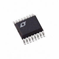
LTC3830EGN Linear Technology, LTC3830EGN Datasheet - Page 18

LTC3830EGN
Manufacturer Part Number
LTC3830EGN
Description
IC DC/DC CONTRLR STEP-DWN 16SSOP
Manufacturer
Linear Technology
Type
Step-Down (Buck)r
Datasheet
1.LTC3830ES8.pdf
(24 pages)
Specifications of LTC3830EGN
Internal Switch(s)
No
Synchronous Rectifier
Yes
Number Of Outputs
1
Voltage - Output
3.3V, Adj
Current - Output
20A
Frequency - Switching
200kHz
Voltage - Input
3 ~ 8 V
Operating Temperature
-40°C ~ 85°C
Mounting Type
Surface Mount
Package / Case
16-SSOP
Lead Free Status / RoHS Status
Contains lead / RoHS non-compliant
Power - Output
-
Available stocks
Company
Part Number
Manufacturer
Quantity
Price
Company:
Part Number:
LTC3830EGN
Manufacturer:
LT
Quantity:
10 000
Part Number:
LTC3830EGN
Manufacturer:
LINEAR
Quantity:
20 000
Company:
Part Number:
LTC3830EGN-8
Manufacturer:
LT
Quantity:
10 000
LTC3830/LTC3830-1
APPLICATIO S I FOR ATIO
Table 3 shows the suggested compensation component
values for 5V to 3.3V applications based on 470µF Sanyo
POSCAP 4TPB470M output capacitors.
Table 3. Recommended Compensation Network for 5V to 3.3V
Applications Using Multiple Paralleled 470µF Sanyo POSCAP
4TPB470M Output Capacitors
Table 4 shows the suggested compensation component
values for 5V to 3.3V applications based on 1500µF Sanyo
MV-WX output capacitors.
Table 4. Recommended Compensation Network for 5V to 3.3V
Applications Using Multiple Paralleled 1500µF Sanyo MV-WX
Output Capacitors
18
L1 (µH)
L1 (µH)
1.2
1.2
1.2
2.4
2.4
2.4
4.7
4.7
4.7
1.2
1.2
1.2
2.4
2.4
2.4
4.7
4.7
4.7
C
C
OUT
OUT
1410
2820
4700
1410
2820
4700
1410
2820
4700
4500
6000
9000
4500
6000
9000
4500
6000
9000
(µF)
(µF)
U
U
R
R
C
C
150
100
150
200
6.8
15
22
18
43
62
43
91
22
30
39
51
62
82
(kΩ)
(kΩ)
W
C
C
C
C
0.47
0.47
0.47
0.47
4.7
2.2
2.2
2.2
2.2
1.5
3.3
10
10
33
10
1
1
1
(nF)
(nF)
U
C1 (pF)
C1 (pF)
120
33
33
33
33
33
10
10
10
10
82
56
56
33
27
15
15
15
LAYOUT CONSIDERATIONS
When laying out the printed circuit board, use the follow-
ing checklist to ensure proper operation of the LTC3830.
These items are also illustrated graphically in the layout
diagram of Figure 11. The thicker lines show the high
current paths. Note that at 10A current levels or above,
current density in the PC board itself is a serious concern.
Traces carrying high current should be as wide as pos-
sible. For example, a PCB fabricated with 2oz copper
requires a minimum trace width of 0.15" to carry 10A.
1. In general, layout should begin with the location of the
power devices. Be sure to orient the power circuitry so that
a clean power flow path is achieved. Conductor widths
should be maximized and lengths minimized. After you are
satisfied with the power path, the control circuitry should
be laid out. It is much easier to find routes for the relatively
small traces in the control circuits than it is to find
circuitous routes for high current paths.
2. The GND and PGND pins should be shorted directly at
the LTC3830. This helps to minimize internal ground dis-
turbances in the LTC3830 and prevent differences in ground
potential from disrupting internal circuit operation. This
connection should then tie into the ground plane at a single
point, preferably at a fairly quiet point in the circuit such as
close to the output capacitors. This is not always practical,
however, due to physical constraints. Another reasonably
good point to make this connection is between the output
capacitors and the source connection of the bottom
MOSFET Q2. Do not tie this single point ground in the trace
run between the Q2 source and the input capacitor ground,
as this area of the ground plane will be very noisy.
3830fa


