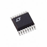
LTC3830EGN Linear Technology, LTC3830EGN Datasheet

LTC3830EGN
Specifications of LTC3830EGN
Available stocks
Related parts for LTC3830EGN
LTC3830EGN Summary of contents
Page 1
... In shutdown mode, the LTC3830 supply current drops to <10µA. The LTC3830-1 differs from the LTC3830 S8 ver- sion by replacing shutdown with a soft-start function. For a similar, pin compatible DC/DC converter with an output voltage as low as 0.6V, please refer to the LTC3832. , LTC and LT are registered trademarks of Linear Technology Corporation 220µF ...
Page 2
... 5V, unless otherwise noted. (Note CC1 CC2 CONDITIONS (Note 1.25V COMP V = 1.25V COMP 10A (Note 6) OUT V = 4.75V to 5.25V CC ORDER PART NUMBER TOP VIEW LTC3830EGN LTC3830ES CC2 PART MARKING MAX 6 11 FREQSET 3830 ...
Page 3
ELECTRICAL CHARACTERISTICS range, otherwise specifications are at T SYMBOL PARAMETER I Supply Current VCC I PV Supply Current PVCC CC f Internal Oscillator Frequency OSC Minimum Duty Cycle SAWL COMP Maximum Duty Cycle SAWH ...
Page 4
LTC3830/LTC3830 TYPICAL PERFOR A CE CHARACTERISTICS Load Regulation 3. 25°C A REFER TO FIGURE 12 3.33 3.32 3.31 3.30 3.29 3.28 3.27 3.26 –10 – –15 0 OUTPUT CURRENT (A) 3830 G02 Output ...
Page 5
W U TYPICAL PERFOR A CE CHARACTERISTICS Maximum G1 Duty Cycle vs Temperature 100 REFER TO FIGURE –50 – 125 50 75 100 TEMPERATURE ...
Page 6
LTC3830/LTC3830 TYPICAL PERFOR A CE CHARACTERISTICS PV Supply Current CC vs Gate Capacitance 25° 12V CC1 CC1 ...
Page 7
CTIO S FREQSET (Pin 11/NA/NA): Frequency Set. Use this pin to adjust the free-running frequency of the internal oscillator. With the pin floating, the oscillator runs at about 200kHz. A resistor from FREQSET to ground ...
Page 8
LTC3830/LTC3830-1 TEST CIRCUITS SHDN CC SHDN CC2 CC1 FREQSET LTC3830 NC COMP I MAX – GND PGND SENSE SENSE Figure APPLICATIO S I FOR ...
Page 9
U U APPLICATIO S I FOR ATIO Similarly, the MAX comparator forces the output to 0% duty cycle if the feedback signal is greater than 40mV above the internal reference. To prevent these two com- parators from triggering due to ...
Page 10
LTC3830/LTC3830 APPLICATIO S I FOR ATIO The usually increases with temperature. To DS(ON) keep the current limit threshold constant, the internal 12µA sink current designed with a positive MAX temperature coefficient to ...
Page 11
U U APPLICATIO S I FOR ATIO External Clock Synchronization The LTC3830 SHDN pin doubles as an external clock input for applications that require a synchronized clock. An internal circuit forces the LTC3830 into external synchro- nization mode if a ...
Page 12
LTC3830/LTC3830 APPLICATIO S I FOR ATIO Input Supply Considerations/Charge Pump The 16-lead LTC3830 requires four supply voltages to operate: V for the main power input MOSFET gate drive and a clean, low ripple V LTC3830 internal ...
Page 13
U U APPLICATIO S I FOR ATIO The LTC3830/LTC3830-1 overcomes this problem by sensing the PV voltage when G1 is high CC1 than (V + 2.5V), the maximum G1 duty cycle is reduced CC to 70% by clamping ...
Page 14
LTC3830/LTC3830 APPLICATIO S I FOR ATIO P should be calculated based primarily on required MAX efficiency or allowable thermal dissipation. A typical high efficiency circuit designed for 5V input and 3.3V at 10A output might allow no more ...
Page 15
U U APPLICATIO S I FOR ATIO where L is the inductor value in µH. With proper fre- O quency compensation, the combination of the inductor and output capacitor values determine the transient recov- ery time. In general, a smaller ...
Page 16
LTC3830/LTC3830 APPLICATIO S I FOR ATIO The output capacitor in a buck converter under steady- state conditions sees much less ripple current than the input capacitor. Peak-to-peak current is equal to inductor ripple current, usually 10% to 40% ...
Page 17
U U APPLICATIO S I FOR ATIO Figure 10b shows the Bode plot of the overall transfer function. When low ESR output capacitors (Sanyo OS-CON) are used, the ESR zero can be high enough in frequency that it provides little ...
Page 18
LTC3830/LTC3830 APPLICATIO S I FOR ATIO Table 3 shows the suggested compensation component values for 5V to 3.3V applications based on 470µF Sanyo POSCAP 4TPB470M output capacitors. Table 3. Recommended Compensation Network for 5V to 3.3V Applications Using ...
Page 19
U U APPLICATIO S I FOR ATIO 3. The small-signal resistors and capacitors for frequency compensation and soft-start should be located very close to their respective pins and the ground ends connected to the signal ground pin through a separate ...
Page 20
LTC3830/LTC3830 APPLICATIO S I FOR ATIO 5V MBR0530T1 + 100Ω 1µ CC2 CC1 + 0.1µF 4.7µ MAX 0.01µF I LTC3830 FB NC FREQSET G2 SHUTDOWN SHDN PGND COMP GND C1 R ...
Page 21
PACKAGE DESCRIPTIO .254 MIN .0165 ± .0015 RECOMMENDED SOLDER PAD LAYOUT .007 – .0098 (0.178 – 0.249) .016 – .050 (0.406 – 1.270) NOTE: 1. CONTROLLING DIMENSION: INCHES INCHES 2. DIMENSIONS ARE IN (MILLIMETERS) 3. DRAWING NOT TO SCALE *DIMENSION ...
Page 22
LTC3830/LTC3830-1 PACKAGE DESCRIPTIO .050 BSC .245 MIN .030 ±.005 TYP RECOMMENDED SOLDER PAD LAYOUT .010 – .020 (0.254 – 0.508) .008 – .010 (0.203 – 0.254) NOTE: 1. DIMENSIONS IN 2. DRAWING NOT TO SCALE 3. THESE DIMENSIONS DO NOT ...
Page 23
... MOLD FLASH OR PROTRUSIONS SHALL NOT EXCEED .006" (0.15mm) Information furnished by Linear Technology Corporation is believed to be accurate and reliable. However, no responsibility is assumed for its use. Linear Technology Corporation makes no represen- tation that the interconnection of its circuits as described herein will not infringe on existing patent rights. ...
Page 24
... Fast DC/DC Step-Down Synchronous Controller with Margining, Tracking and PLL LTC3831 High Power Synchronous Switching Regulator Controller for DDR Memory Termination LTC3832 Synchronous Step-Down Controller trademark of Linear Technology Corporation. SENSE Linear Technology Corporation 24 1630 McCarthy Blvd., Milpitas, CA 95035-7417 (408) 432-1900 FAX: (408) 434-0507 ● ...


