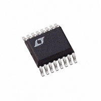
LTC3830EGN Linear Technology, LTC3830EGN Datasheet - Page 13

LTC3830EGN
Manufacturer Part Number
LTC3830EGN
Description
IC DC/DC CONTRLR STEP-DWN 16SSOP
Manufacturer
Linear Technology
Type
Step-Down (Buck)r
Datasheet
1.LTC3830ES8.pdf
(24 pages)
Specifications of LTC3830EGN
Internal Switch(s)
No
Synchronous Rectifier
Yes
Number Of Outputs
1
Voltage - Output
3.3V, Adj
Current - Output
20A
Frequency - Switching
200kHz
Voltage - Input
3 ~ 8 V
Operating Temperature
-40°C ~ 85°C
Mounting Type
Surface Mount
Package / Case
16-SSOP
Lead Free Status / RoHS Status
Contains lead / RoHS non-compliant
Power - Output
-
Available stocks
Company
Part Number
Manufacturer
Quantity
Price
Company:
Part Number:
LTC3830EGN
Manufacturer:
LT
Quantity:
10 000
Part Number:
LTC3830EGN
Manufacturer:
LINEAR
Quantity:
20 000
Company:
Part Number:
LTC3830EGN-8
Manufacturer:
LT
Quantity:
10 000
APPLICATIO S I FOR ATIO
The LTC3830/LTC3830-1 overcomes this problem by
sensing the PV
than (V
to 70% by clamping the COMP pin at 1.8V (QC in BLOCK
DIAGRAM). This increases the G2 on time and allows the
charge pump capacitor to be refreshed.
For Applications using an external supply to power PV
this supply must also be higher than V
to insure normal operation.
For applications with a 5V or higher V
be tied to V
supplied using a doubling charge pump as shown in Figure
9. This circuit provides 2V
Figure 12 shows a typical 5V to 3.3V application using a
doubling charge pump to generate PV
Power MOSFETs
Two N-channel power MOSFETs are required for most
LTC3830 circuits. These should be selected based
primarily on threshold voltage and on-resistance consid-
erations. Thermal dissipation is often a secondary con-
cern in high efficiency designs. The required MOSFET
threshold should be determined based on the available
power supply voltages and/or the complexity of the gate
drive charge pump scheme. In 3.3V input designs where
USE FOR V
D
12V
1N5242
OPTIONAL
Z
CC
IN
+ 2.5V), the maximum G1 duty cycle is reduced
≥ 7V
IN
LTC3830
if a logic level MOSFET is used. PV
Figure 9. Doubling Charge Pump
PV
CC1
CC2
voltage when G1 is high. If PV
U
PV
CC1
G1
G2
U
IN
– V
MBR0530T1
0.1µF
F
to PV
W
IN
V
CC1
IN
CC1
CC
supply, PV
Q1
Q2
by at least 2.5V
.
while Q1 is ON.
L
O
U
CC1
CC1
+
CC2
can be
is less
3830 F09
C
OUT
CC1
can
V
OUT
,
an auxiliary 12V supply is available to power PV
PV
= 5V or 6V can be used with good results. The current
drawn from this supply varies with the MOSFETs used
and the LTC3830’s operating frequency, but is generally
less than 50mA.
LTC3830 applications that use 5V or lower V
a doubling/tripling charge pump to generate PV
PV
enhance standard power MOSFETs. Under this condition,
the effective MOSFET R
the dissipation in the FETs and reducing efficiency. Logic
level FETs are the recommended choice for 5V or lower
voltage systems. Logic level FETs can be fully enhanced
with a doubler/tripling charge pump and will operate at
maximum efficiency.
After the MOSFET threshold voltage is selected, choose the
R
allowable power dissipation and maximum output current.
In a typical LTC3830 circuit, operating in continuous mode,
the average inductor current is equal to the output load
current. This current flows through either Q1 or Q2 with the
power dissipation split up according to the duty cycle:
The R
be calculated by rearranging the relation P = I
R
R
DS(ON)
DS ON Q
DS ON Q
CC2
CC2
DC Q
DC Q
(
(
DS(ON)
( )
(
, do not provide enough gate drive voltage to fully
, standard MOSFETs with R
)
)
1
2
based on the input voltage, the output voltage,
1
2
)
=
=
=
=
required for a given conduction loss can now
V
1
DC Q
DC Q
V
OUT
–
IN
( ) • (
(
V
P
V
P
OUT
MAX Q
1
IN
MAX Q
2
LTC3830/LTC3830-1
) • (
=
( )
I
(
LOAD
I
DS(ON)
LOAD
1
2
V
)
IN
)
–
V
)
2
2
IN
may be quite high, raising
V
=
OUT
=
V
DS(ON)
(
V
OUT
V
IN
IN
•
V
–
P
• (
IN
MAX Q
specified at V
V
I
LOAD
OUT
•
IN
P
( )
MAX Q
voltage and
2
) • (
1
R.
)
2
CC1
CC1
(
13
I
LOAD
2
)
3830fa
and
and
GS
)
2


